Home > Press > Selective CVD growth of GeSn: a new approach for implementing stress in Ge based MOSFETs
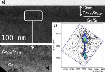 |
| Cross-section TEM and 224 XRD-RSM of fully strained defect-free GeSn layers grown on a Ge substrate. |
Abstract:
Imec reports for the first time selective chemical vapor deposition (CVD) of GeSn in a production-like environment using commercially available Ge and Sn precursors. The resulting GeSn layers with 8% Sn are defect free, fully strained and thermally stable for temperatures up to 500°C. This technique is used to implement uniaxial compressive stress in a Ge channel, the key method for reaching very high mobility values in MOSFETs.
Selective CVD growth of GeSn: a new approach for implementing stress in Ge based MOSFETs
Leuven, Belgium | Posted on August 23rd, 2011Ge as a high mobility channel material has attracted much interest for future CMOS applications where it could potentially replace Si in pMOSFETs. High mobility values can be obtained by stress engineering in the Ge channel. Imec now presents an innovative concept for implementing uniaxial compressive stress in Ge channels by boron doped selective epitaxial growth of GeSn CVD in embedded source/drain areas*. The technique has been demonstrated in a 200mm production-like environment, and is expected to be easily transferable into a 300mm environment.
Key of this technique is a new approach for growing GeSn in a CVD environment. CVD growth of GeSn has so far only been reported by using SnD4 as a Sn gas precursor, but the instability of this precursor restricts the applicability of the technique. Imec uses the stable SnCl4 and Ge2H6 as commercially available Sn and Ge precursors respectively. This permits the growth of GeSn layers on a Ge surface with Sn content up to 8%. As shown by transmission electron microscopy (TEM), no defects are found in the 40nm GeSn layer and according to x-ray diffraction reciprocal space mapping (XRD-RSM) measurements, the layer is fully strained. The GeSn layer grown with this approach survives to further thermal treatments at temperatures up 500°C (for 10 minutes). In addition, in-situ boron (B) doped GeSn CVD growth was investigated by using a combination of Ge2H6, SnCl4 and B2H6 precursors. B was found to be 100% electrically active in GeSn:B layers grown with a B concentration of 1.7e19cm-3.
The CVD grown GeSn layer can also be used as a high-mobility channel material on Ge. A strained GeSn channel on Ge is a possible candidate to be used in the device channel of future Ge based MOSFET devices. In this work, first working GeSn capacitors were realized by depositing Al2O3 on the CVD grown GeSn layers**.
The CVD growth of GeSn with commercially available precursors will boost the research on high-mobility MOSFETs. Besides, it opens new routes for group-IV semiconductors research in other fields, such as photonics (having indirect-to-direct-bandgap transition expected for about 10% Sn incorporated in monocrystalline GeSn allys) and photovoltaics (ternary SiGeSn alloys).
More detailed results can be found in *B. Vincent et al., Microelec. Eng. 88 (2011) 342 and in **B. Vincent et al., Electrochem. Soc. Trans. 2011 (accepted for publication).
####
About IMEC
Imec performs world-leading research in nano-electronics. Imec leverages its scientific knowledge with the innovative power of its global partnerships in ICT, healthcare and energy. Imec delivers industry-relevant technology solutions. In a unique high-tech environment, its international top talent is committed to providing the building blocks for a better life in a sustainable society.
Imec is headquartered in Leuven, Belgium, and has offices in Belgium, the Netherlands, Taiwan, USA, China and Japan. Its staff of about 1,900 people includes more than 500 industrial residents and guest researchers. In 2010, imec's revenue (P&L) was 285 million euro.
Imec is a registered trademark for the activities of IMEC International (a legal entity set up under Belgian law as a "stichting van openbaar nut”), imec Belgium (IMEC vzw supported by the Flemish Government), imec the Netherlands (Stichting IMEC Nederland, part of Holst Centre which is supported by the Dutch Government), imec Taiwan (IMEC Taiwan Co.) and imec China (IMEC Microelectronics (Shangai) Co. Ltd.).
For more information, please click here
Contacts:
Hanne Degans
External Communications Officer
T: +32 16 281 769
Mobile: +32 486 065 175
Copyright © IMEC
If you have a comment, please Contact us.Issuers of news releases, not 7th Wave, Inc. or Nanotechnology Now, are solely responsible for the accuracy of the content.
Bookmark:


| Related News Press |
News and information
![]() Simulating magnetization in a Heisenberg quantum spin chain April 5th, 2024
Simulating magnetization in a Heisenberg quantum spin chain April 5th, 2024
![]() NRL charters Navy’s quantum inertial navigation path to reduce drift April 5th, 2024
NRL charters Navy’s quantum inertial navigation path to reduce drift April 5th, 2024
![]() Discovery points path to flash-like memory for storing qubits: Rice find could hasten development of nonvolatile quantum memory April 5th, 2024
Discovery points path to flash-like memory for storing qubits: Rice find could hasten development of nonvolatile quantum memory April 5th, 2024
Chip Technology
![]() Discovery points path to flash-like memory for storing qubits: Rice find could hasten development of nonvolatile quantum memory April 5th, 2024
Discovery points path to flash-like memory for storing qubits: Rice find could hasten development of nonvolatile quantum memory April 5th, 2024
![]() Utilizing palladium for addressing contact issues of buried oxide thin film transistors April 5th, 2024
Utilizing palladium for addressing contact issues of buried oxide thin film transistors April 5th, 2024
![]() HKUST researchers develop new integration technique for efficient coupling of III-V and silicon February 16th, 2024
HKUST researchers develop new integration technique for efficient coupling of III-V and silicon February 16th, 2024
Discoveries
![]() Chemical reactions can scramble quantum information as well as black holes April 5th, 2024
Chemical reactions can scramble quantum information as well as black holes April 5th, 2024
![]() New micromaterial releases nanoparticles that selectively destroy cancer cells April 5th, 2024
New micromaterial releases nanoparticles that selectively destroy cancer cells April 5th, 2024
![]() Utilizing palladium for addressing contact issues of buried oxide thin film transistors April 5th, 2024
Utilizing palladium for addressing contact issues of buried oxide thin film transistors April 5th, 2024
Announcements
![]() NRL charters Navy’s quantum inertial navigation path to reduce drift April 5th, 2024
NRL charters Navy’s quantum inertial navigation path to reduce drift April 5th, 2024
![]() Discovery points path to flash-like memory for storing qubits: Rice find could hasten development of nonvolatile quantum memory April 5th, 2024
Discovery points path to flash-like memory for storing qubits: Rice find could hasten development of nonvolatile quantum memory April 5th, 2024
Tools
![]() Ferroelectrically modulate the Fermi level of graphene oxide to enhance SERS response November 3rd, 2023
Ferroelectrically modulate the Fermi level of graphene oxide to enhance SERS response November 3rd, 2023
![]() The USTC realizes In situ electron paramagnetic resonance spectroscopy using single nanodiamond sensors November 3rd, 2023
The USTC realizes In situ electron paramagnetic resonance spectroscopy using single nanodiamond sensors November 3rd, 2023
|
|
||
|
|
||
| The latest news from around the world, FREE | ||
|
|
||
|
|
||
| Premium Products | ||
|
|
||
|
Only the news you want to read!
Learn More |
||
|
|
||
|
Full-service, expert consulting
Learn More |
||
|
|
||