Home > Press > Etch-a-sketch with superconductors: A breakthrough in controlling defects could lead to new generation of electronic devices
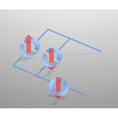 |
| In future, X-ray beams could be used to write superconducting circuits, such as those depicted in the image. Here, solid lines indicate electrical connections while semicircles denote superconducting junctions, whose states are indicated by red arrows.
Credit: UCL Press Office |
Abstract:
Reporting in Nature Materials this week, researchers from the London Centre for Nanotechnology and the Physics Department of Sapienza University of Rome have discovered a technique to 'draw' superconducting shapes using an X-ray beam. This ability to create and control tiny superconducting structures has implications for a completely new generation of electronic devices.
Etch-a-sketch with superconductors: A breakthrough in controlling defects could lead to new generation of electronic devices
London, UK | Posted on August 22nd, 2011Superconductivity is a special state where a material conducts electricity with no resistance, meaning absolutely zero energy is wasted.
The research group has shown that they can manipulate regions of high temperature superconductivity, in a particular material which combines oxygen, copper and a heavier, 'rare earth' element called lanthanum. Illuminating with X-rays causes a small scale re-arrangement of the oxygen atoms in the material, resulting in high temperature superconductivity, of the type originally discovered for such materials 25 years ago by IBM scientists. The X-ray beam is then used like a pen to draw shapes in two dimensions.
A well as being able to write superconductors with dimensions much smaller than the width of a human hair, the group is able to erase those structures by applying heat treatments. They now have the tools to write and erase with high precision, using just a few simple steps and without the chemicals ordinarily used in device fabrication. This ability to re-arrange the underlying structure of a material has wider applications to similar compounds containing metal atoms and oxygen, ranging from fuel cells to catalysts.
Prof. Aeppli, Director of the London Centre for Nanotechnology and the UCL investigator on the project, said: "Our validation of a one-step, chemical-free technique to generate superconductors opens up exciting new possibilities for electronic devices, particularly in re-writing superconducting logic circuits. Of profound importance is the key to solving the notorious 'travelling salesman problem', which underlies many of the world's great computational challenges. We want to create computers on demand to solve this problem, with applications from genetics to logistics. A discovery like this means a paradigm shift in computing technology is one step closer."
Prof Bianconi, the leader of the team from Sapienza, added: "It is amazing that in a few simple steps, we can now add superconducting 'intelligence' directly to a material consisting mainly of the common elements copper and oxygen."
The X-ray experiments were performed at the Elettra (Trieste) synchrotron radiation facility. The work is published in Nature Materials, 21 August 2011 (doi:1038/nmat3088) and follows on from previous discovery of fractal-like structures in superconductors (doi:10.1038/nature09260).
####
For more information, please click here
Contacts:
Dave Weston
44-020-310-83844
Copyright © University College London
If you have a comment, please Contact us.Issuers of news releases, not 7th Wave, Inc. or Nanotechnology Now, are solely responsible for the accuracy of the content.
Bookmark:


| Related News Press |
News and information
![]() Simulating magnetization in a Heisenberg quantum spin chain April 5th, 2024
Simulating magnetization in a Heisenberg quantum spin chain April 5th, 2024
![]() NRL charters Navy�s quantum inertial navigation path to reduce drift April 5th, 2024
NRL charters Navy�s quantum inertial navigation path to reduce drift April 5th, 2024
![]() Discovery points path to flash-like memory for storing qubits: Rice find could hasten development of nonvolatile quantum memory April 5th, 2024
Discovery points path to flash-like memory for storing qubits: Rice find could hasten development of nonvolatile quantum memory April 5th, 2024
Superconductivity
![]() Optically trapped quantum droplets of light can bind together to form macroscopic complexes March 8th, 2024
Optically trapped quantum droplets of light can bind together to form macroscopic complexes March 8th, 2024
![]() 'Sudden death' of quantum fluctuations defies current theories of superconductivity: Study challenges the conventional wisdom of superconducting quantum transitions January 12th, 2024
'Sudden death' of quantum fluctuations defies current theories of superconductivity: Study challenges the conventional wisdom of superconducting quantum transitions January 12th, 2024
![]() Researchers at Purdue discover superconductive images are actually 3D and disorder-driven fractals May 12th, 2023
Researchers at Purdue discover superconductive images are actually 3D and disorder-driven fractals May 12th, 2023
Chip Technology
![]() Discovery points path to flash-like memory for storing qubits: Rice find could hasten development of nonvolatile quantum memory April 5th, 2024
Discovery points path to flash-like memory for storing qubits: Rice find could hasten development of nonvolatile quantum memory April 5th, 2024
![]() Utilizing palladium for addressing contact issues of buried oxide thin film transistors April 5th, 2024
Utilizing palladium for addressing contact issues of buried oxide thin film transistors April 5th, 2024
![]() HKUST researchers develop new integration technique for efficient coupling of III-V and silicon February 16th, 2024
HKUST researchers develop new integration technique for efficient coupling of III-V and silicon February 16th, 2024
Discoveries
![]() Chemical reactions can scramble quantum information as well as black holes April 5th, 2024
Chemical reactions can scramble quantum information as well as black holes April 5th, 2024
![]() New micromaterial releases nanoparticles that selectively destroy cancer cells April 5th, 2024
New micromaterial releases nanoparticles that selectively destroy cancer cells April 5th, 2024
![]() Utilizing palladium for addressing contact issues of buried oxide thin film transistors April 5th, 2024
Utilizing palladium for addressing contact issues of buried oxide thin film transistors April 5th, 2024
Announcements
![]() NRL charters Navy�s quantum inertial navigation path to reduce drift April 5th, 2024
NRL charters Navy�s quantum inertial navigation path to reduce drift April 5th, 2024
![]() Discovery points path to flash-like memory for storing qubits: Rice find could hasten development of nonvolatile quantum memory April 5th, 2024
Discovery points path to flash-like memory for storing qubits: Rice find could hasten development of nonvolatile quantum memory April 5th, 2024
Research partnerships
![]() Discovery points path to flash-like memory for storing qubits: Rice find could hasten development of nonvolatile quantum memory April 5th, 2024
Discovery points path to flash-like memory for storing qubits: Rice find could hasten development of nonvolatile quantum memory April 5th, 2024
![]() Researchers� approach may protect quantum computers from attacks March 8th, 2024
Researchers� approach may protect quantum computers from attacks March 8th, 2024
![]() 'Sudden death' of quantum fluctuations defies current theories of superconductivity: Study challenges the conventional wisdom of superconducting quantum transitions January 12th, 2024
'Sudden death' of quantum fluctuations defies current theories of superconductivity: Study challenges the conventional wisdom of superconducting quantum transitions January 12th, 2024
|
|
||
|
|
||
| The latest news from around the world, FREE | ||
|
|
||
|
|
||
| Premium Products | ||
|
|
||
|
Only the news you want to read!
Learn More |
||
|
|
||
|
Full-service, expert consulting
Learn More |
||
|
|
||