Home > Press > Argonne-pioneered X-ray lens to aid nanomaterials research
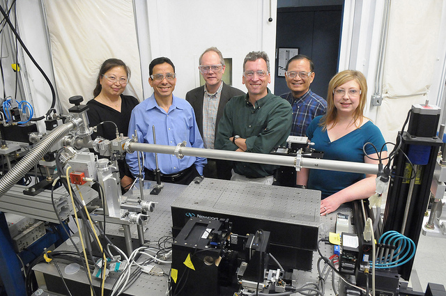 |
| A team of researchers at Argonne has developed the new "multilayer Laue lens," that will let scientists study the nanoscale in greater detail than ever before. From left to right: Bing Shi, Lahsen Assoufid, Brian Stephenson, J�rg Maser, Chian Liu, Lisa Gades. |
Abstract:
More affordable and efficient solar cells, batteries and lighting systems could result from a new X-ray lens that will let scientists study the nanoscale in greater detail than ever before.
Argonne-pioneered X-ray lens to aid nanomaterials research
Argonne, IL | Posted on August 15th, 2011A team of researchers at the U.S. Department of Energy's (DOE) Argonne National Laboratory has developed the new "multilayer Laue lens". This lens focuses high-energy X-rays so tightly they can detect objects as small as 15 nanometers in size and is in principle capable of focusing to well below 10 nanometers. This approach doubles the resolution over existing lenses, and future advancements could increase resolution by 10 times.
Understanding, imaging and manipulating the physical world at the nanoscale is critical to designing materials, devices and technologies that impact our daily lives. To aid in this effort, Argonne's Advanced Photon Source (APS) and Center for Nanoscale Materials (CNM) partnered to improve lens capabilities.
"There's a big need to look into the nanoscale world," said Lahsen Assoufid, Optics Group Leader at the APS. "Availability of this new type of X-ray lens will definitely open new windows into to nanoscale science. "
If you want to look at a material closely�really closely�hard X-rays like those produced at � the APS are the answer. The APS provides some of the nation's brightest beams of X-rays for research; more than 3,500 scientists from industry, academia and national laboratories conducted experiments there last year. These extremely intense and focused X-rays allow scientists to peer into the depths of the nanoworld by focusing the photons on a single small area.
"With this lens, you will be able to see individual nanoparticles," said Argonne physicist J�rg Maser, who conducts research at the APS and CNM." Coupled with the X-rays at the APS, you can detect concentrations of as few as tens of atoms in a complex environment."
The team designed the new lens to improve the focusing of hard X-rays. The lens is crafted by depositing thousands of alternating layers of silicon and tungsten silicide one by one, which are then polished down to just 10 microns thin.
"One of the major 21st century challenges we face is energy," Maser said. "For example, solar energy is not yet cost-effective on a dollar-per-kilowatt-hour level. In order to drive the price down to $1 per kilowatt, we need solar cells that are more efficient and made from less expensive materials. To get there, we need a better understanding of the defects that occur while solar cells are manufactured."
By watching solar cells as they are manufactured and identifying where the defects occur, scientists hope to improve the quality of manufactured cells.
The Argonne team began work on the lens in 2003, working out the complex calculations to predict how�and whether�it would work. Then they needed to demonstrate the idea, perfect a prototype and test the lens. A set of the lenses is now in use at the APS and the CNM, and more are being fabricated. Brookhaven National Laboratory's X-ray synchrotron has begun a strong research effort in fabricating advanced multilayer Laue lenses, Maser said, and groups in Japan and Europe have begun to develop similar systems.
In the near future, the team is expecting to incorporate the new lenses into microelectromechanical systems, or MEMS: mechanical structures with micrometer-size movable parts. MEMS can be used to precisely position and control these new lenses. Particularly attractive is the possibility of automatically focusing the lenses during experiments, and the ability to scan the X-rays very quickly across samples. This research takes place collaboratively between the APS and Argonne's Center for Nanoscale Materials.
This research was supported by the DOE's Office of Basic Energy Sciences. A recent paper on the lens, "Two dimensional hard x-ray nanofocusing with crossed multilayer Laue lenses", was published in Optics Express. The team's deposition approach earned them an R&D100 award in 2005.
The Advanced Photon Source at Argonne National Laboratory is one of five national synchrotron radiation light sources supported by the DOE Office of Science to carry out applied and basic research in order to understand, predict, and ultimately control matter and energy at the electronic, atomic, and molecular levels, provide the foundations for new energy technologies, and support DOE missions in energy, environment, and national security.
The Center for Nanoscale Materials at Argonne National Laboratory is one of the five DOE Nanoscale Science Research Centers (NSRCs), premier national user facilities for interdisciplinary research at the nanoscale, supported by the DOE Office of Science. Together the NSRCs comprise a suite of complementary facilities that provide researchers with state-of-the-art capabilities to fabricate, process, characterize and model nanoscale materials, and constitute the largest infrastructure investment of the National Nanotechnology Initiative. The NSRCs are located at DOE's Argonne, Brookhaven, Lawrence Berkeley, Oak Ridge and Sandia and Los Alamos National Laboratories. For more information about the DOE NSRCs, please visit nano.energy.gov.
By Louise Lerner
####
About Argonne National Laboratory
Argonne National Laboratory seeks solutions to pressing national problems in science and technology. The nation's first national laboratory, Argonne conducts leading-edge basic and applied scientific research in virtually every scientific discipline. Argonne researchers work closely with researchers from hundreds of companies, universities, and federal, state and municipal agencies to help them solve their specific problems, advance America's scientific leadership and prepare the nation for a better future. With employees from more than 60 nations, Argonne is managed by UChicago Argonne, LLC for the U.S. Department of Energy's Office of Science.
For more information, please click here
Contacts:
Louise Lerner
630/252-5526
Copyright © Argonne National Laboratory
If you have a comment, please Contact us.Issuers of news releases, not 7th Wave, Inc. or Nanotechnology Now, are solely responsible for the accuracy of the content.
Bookmark:


| Related Links |
![]() "Two dimensional hard x-ray nanofocusing with crossed multilayer Laue lenses."
"Two dimensional hard x-ray nanofocusing with crossed multilayer Laue lenses."
| Related News Press |
News and information
![]() Simulating magnetization in a Heisenberg quantum spin chain April 5th, 2024
Simulating magnetization in a Heisenberg quantum spin chain April 5th, 2024
![]() NRL charters Navy�s quantum inertial navigation path to reduce drift April 5th, 2024
NRL charters Navy�s quantum inertial navigation path to reduce drift April 5th, 2024
![]() Discovery points path to flash-like memory for storing qubits: Rice find could hasten development of nonvolatile quantum memory April 5th, 2024
Discovery points path to flash-like memory for storing qubits: Rice find could hasten development of nonvolatile quantum memory April 5th, 2024
Imaging
![]() Nanoscale CL thermometry with lanthanide-doped heavy-metal oxide in TEM March 8th, 2024
Nanoscale CL thermometry with lanthanide-doped heavy-metal oxide in TEM March 8th, 2024
Laboratories
![]() A battery�s hopping ions remember where they�ve been: Seen in atomic detail, the seemingly smooth flow of ions through a battery�s electrolyte is surprisingly complicated February 16th, 2024
A battery�s hopping ions remember where they�ve been: Seen in atomic detail, the seemingly smooth flow of ions through a battery�s electrolyte is surprisingly complicated February 16th, 2024
![]() NRL discovers two-dimensional waveguides February 16th, 2024
NRL discovers two-dimensional waveguides February 16th, 2024
Govt.-Legislation/Regulation/Funding/Policy
![]() NRL charters Navy�s quantum inertial navigation path to reduce drift April 5th, 2024
NRL charters Navy�s quantum inertial navigation path to reduce drift April 5th, 2024
![]() Discovery points path to flash-like memory for storing qubits: Rice find could hasten development of nonvolatile quantum memory April 5th, 2024
Discovery points path to flash-like memory for storing qubits: Rice find could hasten development of nonvolatile quantum memory April 5th, 2024
![]() Chemical reactions can scramble quantum information as well as black holes April 5th, 2024
Chemical reactions can scramble quantum information as well as black holes April 5th, 2024
Announcements
![]() NRL charters Navy�s quantum inertial navigation path to reduce drift April 5th, 2024
NRL charters Navy�s quantum inertial navigation path to reduce drift April 5th, 2024
![]() Discovery points path to flash-like memory for storing qubits: Rice find could hasten development of nonvolatile quantum memory April 5th, 2024
Discovery points path to flash-like memory for storing qubits: Rice find could hasten development of nonvolatile quantum memory April 5th, 2024
Tools
![]() Ferroelectrically modulate the Fermi level of graphene oxide to enhance SERS response November 3rd, 2023
Ferroelectrically modulate the Fermi level of graphene oxide to enhance SERS response November 3rd, 2023
![]() The USTC realizes In situ electron paramagnetic resonance spectroscopy using single nanodiamond sensors November 3rd, 2023
The USTC realizes In situ electron paramagnetic resonance spectroscopy using single nanodiamond sensors November 3rd, 2023
Energy
![]() Development of zinc oxide nanopagoda array photoelectrode: photoelectrochemical water-splitting hydrogen production January 12th, 2024
Development of zinc oxide nanopagoda array photoelectrode: photoelectrochemical water-splitting hydrogen production January 12th, 2024
![]() Shedding light on unique conduction mechanisms in a new type of perovskite oxide November 17th, 2023
Shedding light on unique conduction mechanisms in a new type of perovskite oxide November 17th, 2023
![]() Inverted perovskite solar cell breaks 25% efficiency record: Researchers improve cell efficiency using a combination of molecules to address different November 17th, 2023
Inverted perovskite solar cell breaks 25% efficiency record: Researchers improve cell efficiency using a combination of molecules to address different November 17th, 2023
![]() The efficient perovskite cells with a structured anti-reflective layer � another step towards commercialization on a wider scale October 6th, 2023
The efficient perovskite cells with a structured anti-reflective layer � another step towards commercialization on a wider scale October 6th, 2023
Battery Technology/Capacitors/Generators/Piezoelectrics/Thermoelectrics/Energy storage
![]() What heat can tell us about battery chemistry: using the Peltier effect to study lithium-ion cells March 8th, 2024
What heat can tell us about battery chemistry: using the Peltier effect to study lithium-ion cells March 8th, 2024
![]() A battery�s hopping ions remember where they�ve been: Seen in atomic detail, the seemingly smooth flow of ions through a battery�s electrolyte is surprisingly complicated February 16th, 2024
A battery�s hopping ions remember where they�ve been: Seen in atomic detail, the seemingly smooth flow of ions through a battery�s electrolyte is surprisingly complicated February 16th, 2024
Solar/Photovoltaic
![]() Development of zinc oxide nanopagoda array photoelectrode: photoelectrochemical water-splitting hydrogen production January 12th, 2024
Development of zinc oxide nanopagoda array photoelectrode: photoelectrochemical water-splitting hydrogen production January 12th, 2024
![]() Shedding light on unique conduction mechanisms in a new type of perovskite oxide November 17th, 2023
Shedding light on unique conduction mechanisms in a new type of perovskite oxide November 17th, 2023
![]() Inverted perovskite solar cell breaks 25% efficiency record: Researchers improve cell efficiency using a combination of molecules to address different November 17th, 2023
Inverted perovskite solar cell breaks 25% efficiency record: Researchers improve cell efficiency using a combination of molecules to address different November 17th, 2023
![]() Charged �molecular beasts� the basis for new compounds: Researchers at Leipzig University use �aggressive� fragments of molecular ions for chemical synthesis November 3rd, 2023
Charged �molecular beasts� the basis for new compounds: Researchers at Leipzig University use �aggressive� fragments of molecular ions for chemical synthesis November 3rd, 2023
|
|
||
|
|
||
| The latest news from around the world, FREE | ||
|
|
||
|
|
||
| Premium Products | ||
|
|
||
|
Only the news you want to read!
Learn More |
||
|
|
||
|
Full-service, expert consulting
Learn More |
||
|
|
||