Home > Press > CNST Researchers Develop Integrated Nanomechanical Sensor for Atomic Force Microscopy
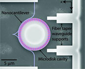 |
| Scanning electron micrograph of the cantilever-microdisksystem. The image has a calculated z-component of the magnetic field overlaid on the structure. |
Abstract:
The atomic force microscope (AFM) is an important tool for nanoscale surface metrology. Typical AFMs map local tip-surface interactions by scanning a flexible cantilever probe over a surface. They rely on bulky optical sensing instrumentation to measure the motion of the probe, which limits the sensitivity, stability, and accuracy of the microscope, and precludes the use of probes much smaller than the wavelength of light. As reported in Nano Letters,* CNST researchers have fabricated a novel integrated sensor combining a nanomechanical cantilever probe with a high sensitivity nanophotonic interferometer on a single silicon chip. Replacing the bulky laser detection system allowed them to build cantilevers orders of magnitude smaller than those used in conventional AFMs.
CNST Researchers Develop Integrated Nanomechanical Sensor for Atomic Force Microscopy
Gaithersburg, MD | Posted on June 6th, 2011Because each of these smaller structures has an effective mass less than a picogram, the detection bandwidth is dramatically increased, reducing the system response time to a few hundred nanoseconds. While probe stiffness was kept comparable to conventional microcantilevers in order to maintain high mechanical gain (how much the tip moves when it senses a force change), the probe size was reduced to a mere 25 �m in length, 260 nm in thickness, and only 65 nm in width. Readout is based on "cavity optomechanics", with the probe fabricated adjacent to a microdisk optical cavity at a gap of less than 100 nm. Due to this close separation, light circulating within the cavity is strongly influenced by the motion of the probe tip. The cavity has a high optical quality factor (Q), meaning that the light makes tens of thousands of round-trips inside the cavity before leaking out of it, all the time accumulating information about the probe's position. The combination of small probe-cavity separation and high Q gives the device sensitivity to probe motion at less than 1 fm/√Hz, while the cavity is able to sense changes in probe position with high bandwidth. The entire device is nanofabricated as a single, monolithic unit on a silicon wafer. It is therefore compact (chip-scale), self-aligned, and stable. Fiber optic waveguides couple light into and out of the sensor, so that it can be easily interfaced with standard optical sources and detectors. Finally, through simple changes to the probe geometry, the mechanics of the probe tip can be greatly varied, allowing for the different combinations of mechanical gain and bandwidth needed for a variety of AFM applications.
*Optomechanical transduction of an integrated silicon cantilever probe using a microdisk resonator, K. Srinivasan, H. Miao, M.T. Rakher, M. Davanco, and V. Aksyuk, Nano Letters 11, 791-797 (2011).
####
About National Institute of Standards and Technology (NIST)
Founded in 1901, NIST is a non-regulatory federal agency within the U.S. Department of Commerce. NIST's mission is to promote U.S. innovation and industrial competitiveness by advancing measurement science, standards, and technology in ways that enhance economic security and improve our quality of life.
For more information, please click here
Contacts:
Kartik Srinivasan
301-975-5938
Copyright © NIST
If you have a comment, please Contact us.Issuers of news releases, not 7th Wave, Inc. or Nanotechnology Now, are solely responsible for the accuracy of the content.
Bookmark:


| Related News Press |
News and information
![]() Simulating magnetization in a Heisenberg quantum spin chain April 5th, 2024
Simulating magnetization in a Heisenberg quantum spin chain April 5th, 2024
![]() NRL charters Navy�s quantum inertial navigation path to reduce drift April 5th, 2024
NRL charters Navy�s quantum inertial navigation path to reduce drift April 5th, 2024
![]() Discovery points path to flash-like memory for storing qubits: Rice find could hasten development of nonvolatile quantum memory April 5th, 2024
Discovery points path to flash-like memory for storing qubits: Rice find could hasten development of nonvolatile quantum memory April 5th, 2024
Imaging
![]() Nanoscale CL thermometry with lanthanide-doped heavy-metal oxide in TEM March 8th, 2024
Nanoscale CL thermometry with lanthanide-doped heavy-metal oxide in TEM March 8th, 2024
Laboratories
![]() A battery�s hopping ions remember where they�ve been: Seen in atomic detail, the seemingly smooth flow of ions through a battery�s electrolyte is surprisingly complicated February 16th, 2024
A battery�s hopping ions remember where they�ve been: Seen in atomic detail, the seemingly smooth flow of ions through a battery�s electrolyte is surprisingly complicated February 16th, 2024
![]() NRL discovers two-dimensional waveguides February 16th, 2024
NRL discovers two-dimensional waveguides February 16th, 2024
Govt.-Legislation/Regulation/Funding/Policy
![]() NRL charters Navy�s quantum inertial navigation path to reduce drift April 5th, 2024
NRL charters Navy�s quantum inertial navigation path to reduce drift April 5th, 2024
![]() Discovery points path to flash-like memory for storing qubits: Rice find could hasten development of nonvolatile quantum memory April 5th, 2024
Discovery points path to flash-like memory for storing qubits: Rice find could hasten development of nonvolatile quantum memory April 5th, 2024
![]() Chemical reactions can scramble quantum information as well as black holes April 5th, 2024
Chemical reactions can scramble quantum information as well as black holes April 5th, 2024
Discoveries
![]() Chemical reactions can scramble quantum information as well as black holes April 5th, 2024
Chemical reactions can scramble quantum information as well as black holes April 5th, 2024
![]() New micromaterial releases nanoparticles that selectively destroy cancer cells April 5th, 2024
New micromaterial releases nanoparticles that selectively destroy cancer cells April 5th, 2024
![]() Utilizing palladium for addressing contact issues of buried oxide thin film transistors April 5th, 2024
Utilizing palladium for addressing contact issues of buried oxide thin film transistors April 5th, 2024
Announcements
![]() NRL charters Navy�s quantum inertial navigation path to reduce drift April 5th, 2024
NRL charters Navy�s quantum inertial navigation path to reduce drift April 5th, 2024
![]() Discovery points path to flash-like memory for storing qubits: Rice find could hasten development of nonvolatile quantum memory April 5th, 2024
Discovery points path to flash-like memory for storing qubits: Rice find could hasten development of nonvolatile quantum memory April 5th, 2024
Tools
![]() Ferroelectrically modulate the Fermi level of graphene oxide to enhance SERS response November 3rd, 2023
Ferroelectrically modulate the Fermi level of graphene oxide to enhance SERS response November 3rd, 2023
![]() The USTC realizes In situ electron paramagnetic resonance spectroscopy using single nanodiamond sensors November 3rd, 2023
The USTC realizes In situ electron paramagnetic resonance spectroscopy using single nanodiamond sensors November 3rd, 2023
|
|
||
|
|
||
| The latest news from around the world, FREE | ||
|
|
||
|
|
||
| Premium Products | ||
|
|
||
|
Only the news you want to read!
Learn More |
||
|
|
||
|
Full-service, expert consulting
Learn More |
||
|
|
||