Home > Press > Seeing an atomic thickness
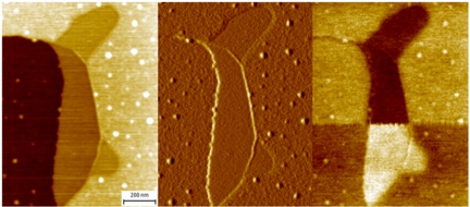 |
| The left hand image is the topography; the middle the topography error image; and right the electrostatic force microscopy image where the tip bias has been switched half way through the image. |
Abstract:
Scientists from NPL, in collaboration with Linköping University, Sweden, have shown that regions of graphene of different thickness can be easily identified in ambient conditions using Electrostatic Force Microscopy (EFM).
Seeing an atomic thickness
UK and Sweden | Posted on May 21st, 2011The exciting properties of graphene are usually only applicable to the material that consists of one or two layers of the graphene sheets. Whilst synthesis of any number of layers is possible, the thicker layers have properties closer to the more common bulk graphite.
For device applications one- and two-layer graphene needs to be precisely identified apart from the substrate and regions of thicker graphene. Exfoliated graphene sheets up to ~100 μm in size can be routinely identified by optical microscopy. However, the situation is much more complicated in the case of the epitaxial graphene grown on silicon carbide wafers with a diameter up to 5 inches where the straightforward identification of the graphene thickness is difficult using standard techniques. This research shows that EFM, which is one of the most widely accessible and simplest implementations of scanning probe microscopy, can clearly identify different graphene thicknesses. The technique can also be used in ambient environments applicable to industrial requirements.
This work was recently published in Nano Letters.
####
About NPL
The National Physical Laboratory (NPL) is one of the UK's leading science and research facilities. It is a world-leading centre of excellence in developing and applying the most accurate standards, science and technology available.
NPL occupies a unique position as the UK's National Measurement Institute and sits at the intersection between scientific discovery and real world application. Its expertise and original research have underpinned quality of life, innovation and competitiveness for UK citizens and business for more than a century:
• NPL provides companies with access to world-leading support and technical expertise, inspiring the absolute confidence required to realise competitive advantage from new materials, techniques and technologies;
• NPL expertise and services are crucial in a wide range of social applications - helping to save lives, protect the environment and enable citizens to feel safe and secure. Support in areas such as the development of advanced medical treatments and environmental monitoring helps secure a better quality of life for all;
• NPL develops and maintains the nation’s primary measurement standards, supporting an infrastructure of traceable measurement throughout the UK and the world, to ensure accuracy and consistency.
For more information, please click here
Contacts:
Dr Tim Burnett
Team Materials
Email
Phone +44 20 8943 8661
Dr Olga Kazakova
Team Time Quantum and Electromagnetics
Email
Phone +44 20 8943 6143
Copyright © NPL
If you have a comment, please Contact us.Issuers of news releases, not 7th Wave, Inc. or Nanotechnology Now, are solely responsible for the accuracy of the content.
Bookmark:


| Related Links |
![]() Find out more about NPL's Functional Materials research.
Find out more about NPL's Functional Materials research.
![]() Find out more about NPL's research into Quantum Phenomena.
Find out more about NPL's research into Quantum Phenomena.
| Related News Press |
News and information
![]() Simulating magnetization in a Heisenberg quantum spin chain April 5th, 2024
Simulating magnetization in a Heisenberg quantum spin chain April 5th, 2024
![]() NRL charters Navy’s quantum inertial navigation path to reduce drift April 5th, 2024
NRL charters Navy’s quantum inertial navigation path to reduce drift April 5th, 2024
![]() Discovery points path to flash-like memory for storing qubits: Rice find could hasten development of nonvolatile quantum memory April 5th, 2024
Discovery points path to flash-like memory for storing qubits: Rice find could hasten development of nonvolatile quantum memory April 5th, 2024
Imaging
![]() Nanoscale CL thermometry with lanthanide-doped heavy-metal oxide in TEM March 8th, 2024
Nanoscale CL thermometry with lanthanide-doped heavy-metal oxide in TEM March 8th, 2024
Graphene/ Graphite
![]() NRL discovers two-dimensional waveguides February 16th, 2024
NRL discovers two-dimensional waveguides February 16th, 2024
Discoveries
![]() Chemical reactions can scramble quantum information as well as black holes April 5th, 2024
Chemical reactions can scramble quantum information as well as black holes April 5th, 2024
![]() New micromaterial releases nanoparticles that selectively destroy cancer cells April 5th, 2024
New micromaterial releases nanoparticles that selectively destroy cancer cells April 5th, 2024
![]() Utilizing palladium for addressing contact issues of buried oxide thin film transistors April 5th, 2024
Utilizing palladium for addressing contact issues of buried oxide thin film transistors April 5th, 2024
Announcements
![]() NRL charters Navy’s quantum inertial navigation path to reduce drift April 5th, 2024
NRL charters Navy’s quantum inertial navigation path to reduce drift April 5th, 2024
![]() Discovery points path to flash-like memory for storing qubits: Rice find could hasten development of nonvolatile quantum memory April 5th, 2024
Discovery points path to flash-like memory for storing qubits: Rice find could hasten development of nonvolatile quantum memory April 5th, 2024
Tools
![]() Ferroelectrically modulate the Fermi level of graphene oxide to enhance SERS response November 3rd, 2023
Ferroelectrically modulate the Fermi level of graphene oxide to enhance SERS response November 3rd, 2023
![]() The USTC realizes In situ electron paramagnetic resonance spectroscopy using single nanodiamond sensors November 3rd, 2023
The USTC realizes In situ electron paramagnetic resonance spectroscopy using single nanodiamond sensors November 3rd, 2023
|
|
||
|
|
||
| The latest news from around the world, FREE | ||
|
|
||
|
|
||
| Premium Products | ||
|
|
||
|
Only the news you want to read!
Learn More |
||
|
|
||
|
Full-service, expert consulting
Learn More |
||
|
|
||