Home > Press > Picosun's plasma enhanced ALD (PEALD) systems sold on three continents
 |
Abstract:
Picosun Oy, Finland-based global manufacturer of state-of-the-art Atomic Layer Deposition (ALD) systems, has launched production of novel, innovative plasma enhanced ALD (PEALD) systems based on highly advanced, customer-proven "ion-free" remote plasma source. Various excited species such as oxygen, nitrogen and hydrogen radicals with zero charge can be generated to broaden the range of ALD process chemistries - especially metal and metal nitride thin films can be deposited at low temperatures with activated species - and the remote source enables processing of even fragile substrates and delicate device structures without plasma damage due to very low ion count but still high reactive species flux.
Picosun's plasma enhanced ALD (PEALD) systems sold on three continents
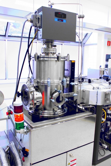
Espoo, Finland | Posted on April 10th, 2011The novel Picoplasma� source system (*) can be mounted on existing SUNALE� ALD reactors or the whole PEALD system can be installed as one compact, small footprint deposition unit of easy implementation, quick maintenance and low cost of ownership. The system can also be fully automated by integrating it into the Picoplatform� cluster tool with cassette-to-cassette loading via a vacuum load lock. Fast matching and stable power delivery of the plasma unit enable high yields with fast process speed and excellent film uniformity (thickness STD 1.3 % with Al2O3 on silicon, deposited from TMA and oxygen radicals) and conformality in deep trenches up to AR of 48:1. In short, the novel Picosplasma� tool increases the already top level versatility, customizability and upscalability of Picosun's existing ALD systems.
ALD was invented by Picosun Board Member Dr. Tuomo Suntola in Finland in the early seventies. Picosun Oy is a Finnish, globally operating manufacturer of state-of-the-art ALD systems for micro- and nanotechnology applications, representing continuity to over three decades of ALD reactor design. Picosun's SUNALE� ALD process tools are used by high profile industries and top research organizations across four continents and the company has redistributors in ca. 30 countries. Picosun Oy is based in Espoo, its manufacturing facilities are located in Kirkkonummi and U.S. headquarters in Detroit, Michigan. Picosun Oy is a part of Stephen Industries Inc Oy.
(*) Multiple patents pending
####
For more information, please click here
Contacts:
Mr. Juhana Kostamo
Phone: +358 50 321 1955
Fax: +358 20 722 7012
E-mail:
Copyright © Picosun Oy
If you have a comment, please Contact us.Issuers of news releases, not 7th Wave, Inc. or Nanotechnology Now, are solely responsible for the accuracy of the content.
Bookmark:


| Related News Press |
News and information
![]() Simulating magnetization in a Heisenberg quantum spin chain April 5th, 2024
Simulating magnetization in a Heisenberg quantum spin chain April 5th, 2024
![]() NRL charters Navy�s quantum inertial navigation path to reduce drift April 5th, 2024
NRL charters Navy�s quantum inertial navigation path to reduce drift April 5th, 2024
![]() Discovery points path to flash-like memory for storing qubits: Rice find could hasten development of nonvolatile quantum memory April 5th, 2024
Discovery points path to flash-like memory for storing qubits: Rice find could hasten development of nonvolatile quantum memory April 5th, 2024
![]() Good as gold - improving infectious disease testing with gold nanoparticles April 5th, 2024
Good as gold - improving infectious disease testing with gold nanoparticles April 5th, 2024
Thin films
![]() Utilizing palladium for addressing contact issues of buried oxide thin film transistors April 5th, 2024
Utilizing palladium for addressing contact issues of buried oxide thin film transistors April 5th, 2024
![]() Understanding the mechanism of non-uniform formation of diamond film on tools: Paving the way to a dry process with less environmental impact March 24th, 2023
Understanding the mechanism of non-uniform formation of diamond film on tools: Paving the way to a dry process with less environmental impact March 24th, 2023
![]() New study introduces the best graphite films: The work by Distinguished Professor Feng Ding at UNIST has been published in the October 2022 issue of Nature Nanotechnology November 4th, 2022
New study introduces the best graphite films: The work by Distinguished Professor Feng Ding at UNIST has been published in the October 2022 issue of Nature Nanotechnology November 4th, 2022
Chip Technology
![]() Discovery points path to flash-like memory for storing qubits: Rice find could hasten development of nonvolatile quantum memory April 5th, 2024
Discovery points path to flash-like memory for storing qubits: Rice find could hasten development of nonvolatile quantum memory April 5th, 2024
![]() Utilizing palladium for addressing contact issues of buried oxide thin film transistors April 5th, 2024
Utilizing palladium for addressing contact issues of buried oxide thin film transistors April 5th, 2024
![]() HKUST researchers develop new integration technique for efficient coupling of III-V and silicon February 16th, 2024
HKUST researchers develop new integration technique for efficient coupling of III-V and silicon February 16th, 2024
Announcements
![]() NRL charters Navy�s quantum inertial navigation path to reduce drift April 5th, 2024
NRL charters Navy�s quantum inertial navigation path to reduce drift April 5th, 2024
![]() Discovery points path to flash-like memory for storing qubits: Rice find could hasten development of nonvolatile quantum memory April 5th, 2024
Discovery points path to flash-like memory for storing qubits: Rice find could hasten development of nonvolatile quantum memory April 5th, 2024
Tools
![]() Ferroelectrically modulate the Fermi level of graphene oxide to enhance SERS response November 3rd, 2023
Ferroelectrically modulate the Fermi level of graphene oxide to enhance SERS response November 3rd, 2023
![]() The USTC realizes In situ electron paramagnetic resonance spectroscopy using single nanodiamond sensors November 3rd, 2023
The USTC realizes In situ electron paramagnetic resonance spectroscopy using single nanodiamond sensors November 3rd, 2023
Patents/IP/Tech Transfer/Licensing
![]() Getting drugs across the blood-brain barrier using nanoparticles March 3rd, 2023
Getting drugs across the blood-brain barrier using nanoparticles March 3rd, 2023
![]() Metasurfaces control polarized light at will: New research unlocks the hidden potential of metasurfaces August 13th, 2021
Metasurfaces control polarized light at will: New research unlocks the hidden potential of metasurfaces August 13th, 2021
![]() Arrowhead Pharmaceuticals Announces Closing of Agreement with Takeda November 27th, 2020
Arrowhead Pharmaceuticals Announces Closing of Agreement with Takeda November 27th, 2020
|
|
||
|
|
||
| The latest news from around the world, FREE | ||
|
|
||
|
|
||
| Premium Products | ||
|
|
||
|
Only the news you want to read!
Learn More |
||
|
|
||
|
Full-service, expert consulting
Learn More |
||
|
|
||