Home > Press > FEI Wins Multi-System Order from CANMET Materials Technology Laboratory
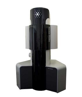 |
| Tecnai Osiris TEM |
Abstract:
Federally-funded research center selects the Tecnai Osiris TEM, Helios NanoLab DualBeam and Nova NanoSEM as part of a competitive evaluation
FEI Wins Multi-System Order from CANMET Materials Technology Laboratory
Hillsboro, OR | Posted on January 5th, 2011FEI Company (NASDAQ: FEIC), a leading instrumentation company providing electron microscope systems for applications in research and industry, today announced that the CANMET Materials Technology Laboratory (CANMET-MTL), a research center funded by the Canadian government, has selected three of FEI's latest electron microscope systems for its new facility at the McMaster Innovation Park, Hamilton, Ontario. As part of a competitive evaluation, CANMET-MTL has purchased the Tecnai Osiris� scanning/transmission electron microscope (S/TEM), the Helios NanoLab� DualBeam�, and the Nova� NanoSEM ultra-high resolution scanning electron microscope (SEM).
According to Tony Edwards, senior vice president for FEI market divisions, "The FEI systems were selected due to a combination of technical capability, price and superior service. CANMET-MTL will have some of the newest, most advanced electron microscopes in its facility."
The Tecnai Osiris S/TEM combines breakthrough analytical throughput with exceptional ease-of-use for high-volume, multi-user research facilities. It features FEI's ChemiSTEM� technology, which reduces the time for large field-of-view elemental mapping from hours to minutes.
The Helios NanoLab DualBeam, the most powerful and versatile DualBeam available today, integrates FEI's extreme high-resolution scanning electron microscope (XHR SEM) with a new, high-performance focused ion beam (FIB), to deliver an unprecedented level of imaging and milling capability. It is designed for research centers that need to perform advanced material characterization and modification down to the single nanometer scale.
FEI's Nova NanoSEM is an ultra-high resolution SEM designed to provide industry-leading nanometer-scale resolution and ultra-precise analysis on the widest range of samples. Adding to this versatility, the system can examine highly insulating samples in low vacuum, with up to nearly the same resolution that can be achieved in high vacuum and with little or no preparation, eliminating artifacts and saving time.
The systems will be shipped to CANMET-MTL in Q1 2011.
For more information, please visit www.fei.com.
FEI Safe Harbor Statement
This news release contains forward-looking statements that include statements regarding the performance capabilities and benefits of the Tecnai Osiris TEM, Helios NanoLab DualBeam, or Nova NanoSEM. Factors that could affect these forward-looking statements include but are not limited to failure of the product or technology to perform as expected and achieve anticipated results, unexpected technology problems and our ability to manufacture, ship and deliver the tools or software as expected. Please also refer to our Form 10-K, Forms 10-Q, Forms 8-K and other filings with the U.S. Securities and Exchange Commission for additional information on these factors and other factors that could cause actual results to differ materially from the forward-looking statements. FEI assumes no duty to update forward-looking statements.
####
About FEI
FEI (Nasdaq: FEIC) is a leading diversified scientific instruments company. It is a premier provider of electron- and ion-beam microscopes and tools for nanoscale applications across many industries: industrial and academic materials research, life sciences, semiconductors, data storage, natural resources and more. With more than 60 years of technological innovation and leadership, FEI has set the performance standard in transmission electron microscopes (TEM), scanning electron microscopes (SEM) and DualBeams�, which combine a SEM with a focused ion beam (FIB). FEI�s imaging systems provide 3D characterization, analysis and modification/prototyping with resolutions down to the sub-�ngstr�m (one-tenth of a nanometer) level. FEI�s NanoPorts in North America, Europe and Asia provide centers of technical excellence where its world-class community of customers and specialists collaborate. FEI has approximately 1800 employees and sales and service operations in more than 50 countries around the world.
For more information, please click here
Contacts:
Sandy Fewkes
MindWrite Communications, Inc.
ph/fx 408.224.4024
www.mind-write.com
Copyright © FEI
If you have a comment, please Contact us.Issuers of news releases, not 7th Wave, Inc. or Nanotechnology Now, are solely responsible for the accuracy of the content.
Bookmark:


| Related News Press |
News and information
![]() Quantum computer improves AI predictions April 17th, 2026
Quantum computer improves AI predictions April 17th, 2026
![]() Flexible sensor gains sensitivity under pressure April 17th, 2026
Flexible sensor gains sensitivity under pressure April 17th, 2026
![]() A reusable chip for particulate matter sensing April 17th, 2026
A reusable chip for particulate matter sensing April 17th, 2026
![]() Detecting vibrational quantum beating in the predissociation dynamics of SF6 using time-resolved photoelectron spectroscopy April 17th, 2026
Detecting vibrational quantum beating in the predissociation dynamics of SF6 using time-resolved photoelectron spectroscopy April 17th, 2026
Announcements
![]() A fundamentally new therapeutic approach to cystic fibrosis: Nanobody repairs cellular defect April 17th, 2026
A fundamentally new therapeutic approach to cystic fibrosis: Nanobody repairs cellular defect April 17th, 2026
![]() UC Irvine physicists discover method to reverse �quantum scrambling� : The work addresses the problem of information loss in quantum computing system April 17th, 2026
UC Irvine physicists discover method to reverse �quantum scrambling� : The work addresses the problem of information loss in quantum computing system April 17th, 2026
Tools
![]() Metasurfaces smooth light to boost magnetic sensing precision January 30th, 2026
Metasurfaces smooth light to boost magnetic sensing precision January 30th, 2026
![]() From sensors to smart systems: the rise of AI-driven photonic noses January 30th, 2026
From sensors to smart systems: the rise of AI-driven photonic noses January 30th, 2026
![]() Japan launches fully domestically produced quantum computer: Expo visitors to experience quantum computing firsthand August 8th, 2025
Japan launches fully domestically produced quantum computer: Expo visitors to experience quantum computing firsthand August 8th, 2025
New-Contracts/Sales/Customers
![]() Bruker Light-Sheet Microscopes at Major Comprehensive Cancer Center: New Advanced Imaging Center Powered by Two MuVi and LCS SPIM Microscopes March 25th, 2021
Bruker Light-Sheet Microscopes at Major Comprehensive Cancer Center: New Advanced Imaging Center Powered by Two MuVi and LCS SPIM Microscopes March 25th, 2021
![]() Arrowhead Pharmaceuticals Announces Closing of Agreement with Takeda November 27th, 2020
Arrowhead Pharmaceuticals Announces Closing of Agreement with Takeda November 27th, 2020
![]() Veeco Announces Aledia Order of 300mm MOCVD Equipment for microLED Displays: Propel� Platform First 300mm System with EFEM Designed for Advanced Display Applications October 20th, 2020
Veeco Announces Aledia Order of 300mm MOCVD Equipment for microLED Displays: Propel� Platform First 300mm System with EFEM Designed for Advanced Display Applications October 20th, 2020
![]() GREENWAVES TECHNOLOGIES Announces Next Generation GAP9 Hearables Platform Using GLOBALFOUNDRIES 22FDX Solution October 16th, 2020
GREENWAVES TECHNOLOGIES Announces Next Generation GAP9 Hearables Platform Using GLOBALFOUNDRIES 22FDX Solution October 16th, 2020
|
|
||
|
|
||
| The latest news from around the world, FREE | ||
|
|
||
|
|
||
| Premium Products | ||
|
|
||
|
Only the news you want to read!
Learn More |
||
|
|
||
|
Full-service, expert consulting
Learn More |
||
|
|
||