Home > Press > Polish scientists present super electron microscope
 |
Abstract:
EU-funded scientists in Poland have completed tests on the TITAN CUBED 80-300, a high-resolution transmission electron microscope.
Polish scientists present super electron microscope
EU | Posted on December 13th, 2010This advanced tool makes it possible for researchers to perform fast and accurate characterisations of semi-conductor structures used in laser and diode productions, and closer testing of materials used in spintronics and nanotechnology.
Partial funding for the project came from the EU's Innovative Economy 'Operational Programme', under the European Regional Development Fund (ERDF). The Innovative Economy scheme supports research and development (R&D) and information and communication technologies (ICT) projects.
The researchers from the Institute of Physics of the Polish Academy of Sciences (PAS) tested and installed the microscope over a four-month period. It is one of the leading facilities found in Europe, according to them.
'Electron microscopy has been the subject of our interest for more than 35 years,' says Professor Leszek Sirko, scientific director of the Institute of Physics. 'TITAN guarantees to carry on our investigation on the highest world level.'
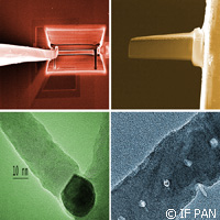
The team says high-resolution transmission electron microscopy (HRTEM) is a valuable tool for researchers wishing to study nanoscale properties of crystalline materials including metals and semi-conductors.
Individual atoms and structural defects can be imaged at these small scales. 'So small objects we are not able to see by use of visible light,' explains Kamil Sobczak, a PhD student at the Institute's Electron Microscopy Group. The team used a beam of electrons instead of a beam of light to 'illuminate' the object.
The microscope consists of a vertical column, on which the electron gun is placed. Once the electron beam has passed through the object, it comes through a system of lenses to create the super magnified image of the object.
According to the team, the object must be very thin (up to one micron, maximum). The group has also picked up a device that enables highly efficient sample thinning, namely a Focus Ion Beam (FIB). 'At present, sample preparation takes us about one week (with standard techniques),' notes Alicja Szczepanska from the Electron Microscopy Group. 'By using an FIB, a sample will be ready after a few hours.'
An electron energy loss spectrometer is included in the state-of-the-art microscope, allowing for holographic imaging and liquid nitrogen temperature testing. The scientists point out that the facility contains high-quality electronic optics, as well as highly stable accelerating voltage and super sensitive image detectors.
The microscope's distinct qualities allow researchers to follow specific processes such as changes in temperature. Researchers will benefit immensely from the microscope, they add.
Based on the results of the microscopic tests 'we will be able to inform technologists, which colour of light can be emitted by a selected part of the investigated device', says Professor Piotr Dluzewski, head of the Electron Microscopy Group.
Regular work of the microscope will get off the ground in January 2011. Scientists and business actors, both in Poland and abroad, are expected to use the new microscope.
For more information, please visit:
Institute of Physics of the Polish Academy of Sciences: www.ifpan.edu.pl/index_en.php
####
For more information, please click here
Copyright © CORDIS
If you have a comment, please Contact us.Issuers of news releases, not 7th Wave, Inc. or Nanotechnology Now, are solely responsible for the accuracy of the content.
Bookmark:


| Related News Press |
News and information
![]() Simulating magnetization in a Heisenberg quantum spin chain April 5th, 2024
Simulating magnetization in a Heisenberg quantum spin chain April 5th, 2024
![]() NRL charters Navy�s quantum inertial navigation path to reduce drift April 5th, 2024
NRL charters Navy�s quantum inertial navigation path to reduce drift April 5th, 2024
![]() Discovery points path to flash-like memory for storing qubits: Rice find could hasten development of nonvolatile quantum memory April 5th, 2024
Discovery points path to flash-like memory for storing qubits: Rice find could hasten development of nonvolatile quantum memory April 5th, 2024
Govt.-Legislation/Regulation/Funding/Policy
![]() NRL charters Navy�s quantum inertial navigation path to reduce drift April 5th, 2024
NRL charters Navy�s quantum inertial navigation path to reduce drift April 5th, 2024
![]() Discovery points path to flash-like memory for storing qubits: Rice find could hasten development of nonvolatile quantum memory April 5th, 2024
Discovery points path to flash-like memory for storing qubits: Rice find could hasten development of nonvolatile quantum memory April 5th, 2024
![]() Chemical reactions can scramble quantum information as well as black holes April 5th, 2024
Chemical reactions can scramble quantum information as well as black holes April 5th, 2024
Academic/Education
![]() Rice University launches Rice Synthetic Biology Institute to improve lives January 12th, 2024
Rice University launches Rice Synthetic Biology Institute to improve lives January 12th, 2024
![]() Multi-institution, $4.6 million NSF grant to fund nanotechnology training September 9th, 2022
Multi-institution, $4.6 million NSF grant to fund nanotechnology training September 9th, 2022
Announcements
![]() NRL charters Navy�s quantum inertial navigation path to reduce drift April 5th, 2024
NRL charters Navy�s quantum inertial navigation path to reduce drift April 5th, 2024
![]() Discovery points path to flash-like memory for storing qubits: Rice find could hasten development of nonvolatile quantum memory April 5th, 2024
Discovery points path to flash-like memory for storing qubits: Rice find could hasten development of nonvolatile quantum memory April 5th, 2024
Tools
![]() Ferroelectrically modulate the Fermi level of graphene oxide to enhance SERS response November 3rd, 2023
Ferroelectrically modulate the Fermi level of graphene oxide to enhance SERS response November 3rd, 2023
![]() The USTC realizes In situ electron paramagnetic resonance spectroscopy using single nanodiamond sensors November 3rd, 2023
The USTC realizes In situ electron paramagnetic resonance spectroscopy using single nanodiamond sensors November 3rd, 2023
|
|
||
|
|
||
| The latest news from around the world, FREE | ||
|
|
||
|
|
||
| Premium Products | ||
|
|
||
|
Only the news you want to read!
Learn More |
||
|
|
||
|
Full-service, expert consulting
Learn More |
||
|
|
||