Home > Press > Vibrating nanorods measure thin films for microcircuits
 |
Abstract:
A key step in many nanofabrication processes is to create thin films, sometimes only one molecule thick, by a method known as atomic layer deposition. Researchers at Cornell and Tel Aviv University have developed a new tool for nanofabricators to test the physical properties of such films.
By Bill Steele
Vibrating nanorods measure thin films for microcircuits
Ithaca, NY | Posted on December 11th, 2010Ultrathin films are increasingly important in constructing microcircuits. Their physical characteristics often determine their electronic behavior as well as their resistance to wear.
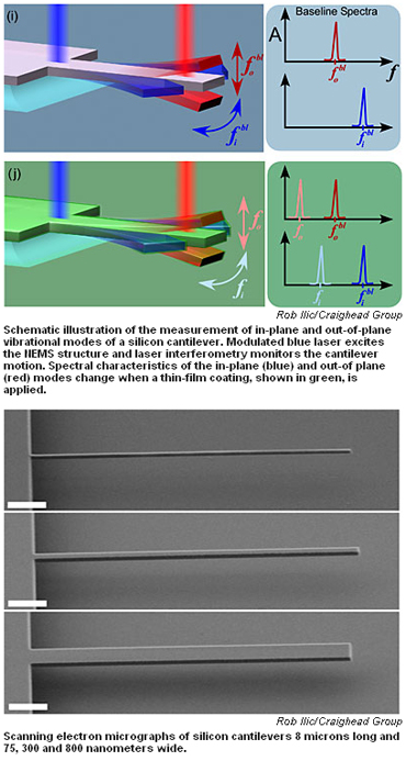
The researchers have shown that tiny resonant cantilevers -- silicon rods anchored at one end, like a tiny diving board -- can determine the density of a film and its Young's modulus, a measure of resistance to bending. The method offers several advantages over other methods of measuring these characteristics of thin films, the researchers said, and can be used by any researchers with access to nanofabrication capabilities comparable to those at the Cornell Nanoscale Facility.
The work was reported in the Aug. 15 issue of the Journal of Applied Physics by Cornell research associate Rob Ilic, Slava Krylov, senior lecturer at Tel Aviv University and former visiting professor at Cornell, and Harold Craighead, the C.W. Lake Jr. Professor of Engineering at Cornell.
Cornell researchers have previously used tiny vibrating cantilevers just a few nanometers (billionths of a meter) thick to detect the mass of objects as small as a virus. Just as a thick guitar string vibrates at a lower note than a thinner one, adding mass to a vibrating rod changes its frequency of vibration. Coating the rod with a thin film adds detectable mass, and from the mass and thickness of the film, density can be determined.
The film also changes the cantilever's resistance to bending. To separate out this characteristic, the researchers compared in-plane (side to side) and out-of-plane (up and down) vibrations. The resistance to bending in different directions is noticeably different when the vibrating rod is wide and thin. When the cross-section of the rod is square, there is no difference between up and down and side-to-side movement.
To test their idea, the researchers fabricated a variety of cantilevers six to 10 microns (millionths of a meter) long, 45 nanometers thick and with widths varying from 45 nanometers to 1 micron. In various experiments, they applied films of aluminum, aluminum nitride and hafnium from 21.2 to 21.5 nanometers thick to the surface of the cantilevers.
A laser beam focused on the base of a cantilever supplies energy to set it vibrating, and another laser aimed at the end measures the vibration. Like a tuning fork, each rod has a resonant frequency at which it vibrates, and that depends on the dimensions and physical characteristics of the device. Comparing the resonant frequency and some of its harmonics before and after a film was applied enabled the researchers to calculate the density and Young's modulus of the film.
Over many experiments, the calculations agreed well with theoretical predictions and characteristics of films measured by other methods. Some aspects of the method of fabricating the nanocantilevers could affect the results, the researchers found, but they said accuracy could be improved.
The work was supported by the Defense Advanced Projects Research Administration, the National Science Foundation and the state of New York.
####
For more information, please click here
Contacts:
Media Contact:
Joe Schwartz
(607) 254-6235
Cornell Chronicle:
Bill Steele
(607) 255-7164
Copyright © Cornell University
If you have a comment, please Contact us.Issuers of news releases, not 7th Wave, Inc. or Nanotechnology Now, are solely responsible for the accuracy of the content.
Bookmark:


| Related News Press |
News and information
![]() Simulating magnetization in a Heisenberg quantum spin chain April 5th, 2024
Simulating magnetization in a Heisenberg quantum spin chain April 5th, 2024
![]() NRL charters Navy�s quantum inertial navigation path to reduce drift April 5th, 2024
NRL charters Navy�s quantum inertial navigation path to reduce drift April 5th, 2024
![]() Discovery points path to flash-like memory for storing qubits: Rice find could hasten development of nonvolatile quantum memory April 5th, 2024
Discovery points path to flash-like memory for storing qubits: Rice find could hasten development of nonvolatile quantum memory April 5th, 2024
![]() Good as gold - improving infectious disease testing with gold nanoparticles April 5th, 2024
Good as gold - improving infectious disease testing with gold nanoparticles April 5th, 2024
Thin films
![]() Utilizing palladium for addressing contact issues of buried oxide thin film transistors April 5th, 2024
Utilizing palladium for addressing contact issues of buried oxide thin film transistors April 5th, 2024
![]() Understanding the mechanism of non-uniform formation of diamond film on tools: Paving the way to a dry process with less environmental impact March 24th, 2023
Understanding the mechanism of non-uniform formation of diamond film on tools: Paving the way to a dry process with less environmental impact March 24th, 2023
![]() New study introduces the best graphite films: The work by Distinguished Professor Feng Ding at UNIST has been published in the October 2022 issue of Nature Nanotechnology November 4th, 2022
New study introduces the best graphite films: The work by Distinguished Professor Feng Ding at UNIST has been published in the October 2022 issue of Nature Nanotechnology November 4th, 2022
Govt.-Legislation/Regulation/Funding/Policy
![]() NRL charters Navy�s quantum inertial navigation path to reduce drift April 5th, 2024
NRL charters Navy�s quantum inertial navigation path to reduce drift April 5th, 2024
![]() Discovery points path to flash-like memory for storing qubits: Rice find could hasten development of nonvolatile quantum memory April 5th, 2024
Discovery points path to flash-like memory for storing qubits: Rice find could hasten development of nonvolatile quantum memory April 5th, 2024
![]() Chemical reactions can scramble quantum information as well as black holes April 5th, 2024
Chemical reactions can scramble quantum information as well as black holes April 5th, 2024
Academic/Education
![]() Rice University launches Rice Synthetic Biology Institute to improve lives January 12th, 2024
Rice University launches Rice Synthetic Biology Institute to improve lives January 12th, 2024
![]() Multi-institution, $4.6 million NSF grant to fund nanotechnology training September 9th, 2022
Multi-institution, $4.6 million NSF grant to fund nanotechnology training September 9th, 2022
Chip Technology
![]() Discovery points path to flash-like memory for storing qubits: Rice find could hasten development of nonvolatile quantum memory April 5th, 2024
Discovery points path to flash-like memory for storing qubits: Rice find could hasten development of nonvolatile quantum memory April 5th, 2024
![]() Utilizing palladium for addressing contact issues of buried oxide thin film transistors April 5th, 2024
Utilizing palladium for addressing contact issues of buried oxide thin film transistors April 5th, 2024
![]() HKUST researchers develop new integration technique for efficient coupling of III-V and silicon February 16th, 2024
HKUST researchers develop new integration technique for efficient coupling of III-V and silicon February 16th, 2024
Nanomedicine
![]() New micromaterial releases nanoparticles that selectively destroy cancer cells April 5th, 2024
New micromaterial releases nanoparticles that selectively destroy cancer cells April 5th, 2024
![]() Good as gold - improving infectious disease testing with gold nanoparticles April 5th, 2024
Good as gold - improving infectious disease testing with gold nanoparticles April 5th, 2024
![]() Researchers develop artificial building blocks of life March 8th, 2024
Researchers develop artificial building blocks of life March 8th, 2024
Announcements
![]() NRL charters Navy�s quantum inertial navigation path to reduce drift April 5th, 2024
NRL charters Navy�s quantum inertial navigation path to reduce drift April 5th, 2024
![]() Discovery points path to flash-like memory for storing qubits: Rice find could hasten development of nonvolatile quantum memory April 5th, 2024
Discovery points path to flash-like memory for storing qubits: Rice find could hasten development of nonvolatile quantum memory April 5th, 2024
Tools
![]() Ferroelectrically modulate the Fermi level of graphene oxide to enhance SERS response November 3rd, 2023
Ferroelectrically modulate the Fermi level of graphene oxide to enhance SERS response November 3rd, 2023
![]() The USTC realizes In situ electron paramagnetic resonance spectroscopy using single nanodiamond sensors November 3rd, 2023
The USTC realizes In situ electron paramagnetic resonance spectroscopy using single nanodiamond sensors November 3rd, 2023
Research partnerships
![]() Discovery points path to flash-like memory for storing qubits: Rice find could hasten development of nonvolatile quantum memory April 5th, 2024
Discovery points path to flash-like memory for storing qubits: Rice find could hasten development of nonvolatile quantum memory April 5th, 2024
![]() Researchers� approach may protect quantum computers from attacks March 8th, 2024
Researchers� approach may protect quantum computers from attacks March 8th, 2024
![]() 'Sudden death' of quantum fluctuations defies current theories of superconductivity: Study challenges the conventional wisdom of superconducting quantum transitions January 12th, 2024
'Sudden death' of quantum fluctuations defies current theories of superconductivity: Study challenges the conventional wisdom of superconducting quantum transitions January 12th, 2024
|
|
||
|
|
||
| The latest news from around the world, FREE | ||
|
|
||
|
|
||
| Premium Products | ||
|
|
||
|
Only the news you want to read!
Learn More |
||
|
|
||
|
Full-service, expert consulting
Learn More |
||
|
|
||