Home > Press > Imaging with neutrons: Magnetic domains shown for the first time in 3D
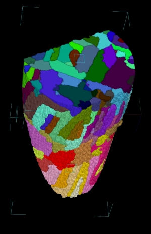 |
| Boundaries of magnetic domains can be computer imaged in three dimensions. Image: HZB/Manke, Grothausmann |
Abstract:
So far, it has only been possible to image magnetic domains in two dimensions. Now, for the first time, Scientists at Helmholtz-Zentrum Berlin (HZB) have managed to create three-dimensional images of these domains deep within magnetic materials.
Imaging with neutrons: Magnetic domains shown for the first time in 3D
Berlin | Posted on November 25th, 2010Although they exist in almost every magnetic material, you cannot see them: magnetic domains are microscopically small regions of uniform magnetization. Every magnetic material is divided into such domains. Scientists call them "Weiss domains" after physicist Pierre-Ernest Weiss, who predicted their existence theoretically more than a hundred years ago. In 1907, he recognized that the magnetic moments of atoms within a bounded domain are equally aligned.
All pursuit of this theory has so far been limited to two-dimensional images and material surfaces. Accordingly, researchers have only ever been able to see a domain in cross section. Together with colleagues from the German Federal Institute for Materials Research and Testing and the Swiss Paul-Scherrer-Institute, Dr. Ingo Manke and his group at the Institute of Applied Material Research at HZB have developed a method by which they can image the full spatial structure of magnetic domains - even deep within materials. To do this, special iron-silicon crystals were produced at the Leibniz Institute for Solid State and Materials Research Dresden, for which the research group of Rudolf Sch�fer had already developed model representations. Their actual existence has now been proven for the first time. With it, the researchers have solved a decade-old problem in imaging. Their findings will be published in Nature Communications (DOI: 10.1038 /ncomms1125).
Most magnetic materials consist of a complex network of magnetic domains. The researchers' newly developed method exploits the areas where the domains meet - the so-called domain walls. Within a domain, all magnetic moments are the same, but the magnetic alignment is different from one domain to another. So, at each domain wall, the direction of the magnetic field changes. The researchers exploit these changes for their radiographic method in which they use not light, but neutrons.
Magnetic fields deflect the neutrons slightly from their flight path, just as water diverts light. An object under water cannot be directly perceived because of this phenomenon; the object appears distorted and in a different location. Similarly, the neutrons pass through domain walls along their path through the magnetic material. At these walls, they are diverted into different directions.
This diversion, however, is only a very weak effect. It is typically invisible in a neutron radiogram, since it is overshadowed by non-diverted rays. The researchers therefore employ several diffraction gratings in order to separate the diverted rays. During a measurement, they rotate the sample and shoot rays through it from all directions. From the separated rays, they can calculate all domain shapes and generate an image of the domain network in its entirety.
Magnetic domains are important for understanding material properties and the natural laws of physics. They also play an important role in everyday life: most notably in storage media such as hard disks, for example, or battery chargers for laptops or electric vehicles. If the domain properties are carefully chosen to minimize electricity loss at the domain walls, the battery charger becomes more efficient.
####
For more information, please click here
Contacts:
Dr. Ingo Manke
(030) 8062 - 42682
(030) 8062 - 43059
Dr. Ina Helms
(030) 8062 - 42034
(030) 8062 - 42998
Copyright © Helmholtz-Zentrum Berlin
If you have a comment, please Contact us.Issuers of news releases, not 7th Wave, Inc. or Nanotechnology Now, are solely responsible for the accuracy of the content.
Bookmark:


| Related News Press |
Physics
![]() Simulating magnetization in a Heisenberg quantum spin chain April 5th, 2024
Simulating magnetization in a Heisenberg quantum spin chain April 5th, 2024
News and information
![]() Simulating magnetization in a Heisenberg quantum spin chain April 5th, 2024
Simulating magnetization in a Heisenberg quantum spin chain April 5th, 2024
![]() NRL charters Navy�s quantum inertial navigation path to reduce drift April 5th, 2024
NRL charters Navy�s quantum inertial navigation path to reduce drift April 5th, 2024
![]() Discovery points path to flash-like memory for storing qubits: Rice find could hasten development of nonvolatile quantum memory April 5th, 2024
Discovery points path to flash-like memory for storing qubits: Rice find could hasten development of nonvolatile quantum memory April 5th, 2024
Academic/Education
![]() Rice University launches Rice Synthetic Biology Institute to improve lives January 12th, 2024
Rice University launches Rice Synthetic Biology Institute to improve lives January 12th, 2024
![]() Multi-institution, $4.6 million NSF grant to fund nanotechnology training September 9th, 2022
Multi-institution, $4.6 million NSF grant to fund nanotechnology training September 9th, 2022
Announcements
![]() NRL charters Navy�s quantum inertial navigation path to reduce drift April 5th, 2024
NRL charters Navy�s quantum inertial navigation path to reduce drift April 5th, 2024
![]() Discovery points path to flash-like memory for storing qubits: Rice find could hasten development of nonvolatile quantum memory April 5th, 2024
Discovery points path to flash-like memory for storing qubits: Rice find could hasten development of nonvolatile quantum memory April 5th, 2024
Tools
![]() Ferroelectrically modulate the Fermi level of graphene oxide to enhance SERS response November 3rd, 2023
Ferroelectrically modulate the Fermi level of graphene oxide to enhance SERS response November 3rd, 2023
![]() The USTC realizes In situ electron paramagnetic resonance spectroscopy using single nanodiamond sensors November 3rd, 2023
The USTC realizes In situ electron paramagnetic resonance spectroscopy using single nanodiamond sensors November 3rd, 2023
Battery Technology/Capacitors/Generators/Piezoelectrics/Thermoelectrics/Energy storage
![]() What heat can tell us about battery chemistry: using the Peltier effect to study lithium-ion cells March 8th, 2024
What heat can tell us about battery chemistry: using the Peltier effect to study lithium-ion cells March 8th, 2024
![]() A battery�s hopping ions remember where they�ve been: Seen in atomic detail, the seemingly smooth flow of ions through a battery�s electrolyte is surprisingly complicated February 16th, 2024
A battery�s hopping ions remember where they�ve been: Seen in atomic detail, the seemingly smooth flow of ions through a battery�s electrolyte is surprisingly complicated February 16th, 2024
|
|
||
|
|
||
| The latest news from around the world, FREE | ||
|
|
||
|
|
||
| Premium Products | ||
|
|
||
|
Only the news you want to read!
Learn More |
||
|
|
||
|
Full-service, expert consulting
Learn More |
||
|
|
||