Home > Press > Singapore’s A*STAR participates in groundbreaking European Union (EU) project to jointly create a processor that is the size of a molecule
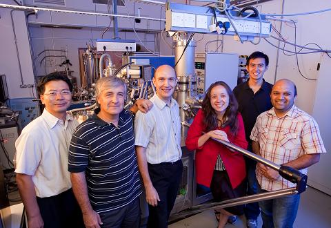 |
| Prof Chirstian Joachim (second from left) and some the Atom Technology team at Singapore A*STAR’s IMRE, which holds the only patent in the world for making solid interconnections and packaging of a molecular chip. |
Abstract:
A*STAR's Institute of Materials Research and Engineering (IMRE) partners 10 EU research organisations to work on the groundbreaking €10 million ATMOL project that lays the foundation for creating and testing a molecular-sized processor chip.
Singapore’s A*STAR participates in groundbreaking European Union (EU) project to jointly create a processor that is the size of a molecule
Singapore | Posted on November 19th, 2010A*STAR's IMRE and 10 EU research organisations are working together to build what is essentially a single molecule processor chip. As a comparison, a thousand of such molecular chips could fit into one of today's microchips, the core device that determines computational speed. The ambitious project, termed Atomic Scale and Single Molecule Logic Gate Technologies (ATMOL), will establish a new process for making a complete molecular chip. This means that computing power can be increased significantly but take up only a small fraction of the space that is required by today's standards.
The fabrication process involves the use of three unique ultra high vacuum (UHV) atomic scale interconnection machines which build the chip atom-by-atom. These machines physically move atoms into place one at a time at cryogenic temperatures. One of these machines is located in A*STAR's IMRE.
"IMRE holds the only patent in the world for making solid interconnections and packaging of a molecular chip", says Prof Christian Joachim, who is leading the entire project, explaining the reason A*STAR's IMRE was chosen as a partner in this groundbreaking project.
"The UHV interconnection machine at IMRE is the only one in the entire project that can study the performance of a single molecule logic gate and surface atom circuit logic gate at the moment", added Prof Joachim, who is the Head of Molecular Nanoscience and Picotechnology at the French Centre National de la Recherche Scientifique (CNRS), and a Visiting Investigator at IMRE. Prof Joachim's team in IMRE is one of the pioneers in atom technology, having built the world's first controllable molecular gear.
"The work in this project is extremely important in setting the stage for how computer chips and electronics may be made in the future", said Prof Andy Hor, Executive Director of IMRE. "The fact that we are the only non-EU research organisation in this project speaks volumes about the level of Singapore's research and how far we have come in building our R&D capabilities".
According to Dr. David Guedj, the European Officer following ATMOL for The European Commission, "ATMOL is the flagship project coming out of the recent Call for Proposals on Molecular Scale Devices and Systems". It was launched by the Future and Emerging Technologies (FET-Proactive) part of the Information and Communication Technologies (ICT) programme of the European Commission. FET-Proactive supports transformational, long-term collaborative frontier research in Europe, with a view to develop scientific excellence and technological innovation.
As part of the project, annual ATMOL conferences will be held to bring together all project partners for progress updates. The inaugural conference will be hosted by Singapore next year. The project will officially commence on 1 January 2011.
####
About A*STAR
The Agency for Science, Technology and Research (A*STAR) is the lead agency for fostering world-class scientific research and talent for a vibrant knowledge-based and innovation-driven Singapore. A*STAR oversees 14 biomedical sciences, and physical sciences and engineering research institutes, and seven consortia & centres, which are located in Biopolis and Fusionopolis, as well as their immediate vicinity.
A*STAR supports Singapore's key economic clusters by providing intellectual, human and industrial capital to its partners in industry. It also supports extramural research in the universities, hospitals, research centres, and with other local and international partners.
For more information about A*STAR, please visit www.a-star.edu.sg
About the Institute of Materials Research and Engineering (IMRE)
Established in September 1997, IMRE has built strong capabilities in materials analysis, characterisation, materials growth, patterning, fabrication, synthesis and integration. IMRE is an institute of talented researchers equipped with state-of-the-art facilities such as the SERC nanofabrication, Processing and Characterisation facility to conduct world-class materials science research. Leveraging on these capabilities, R&D programmes have been established in collaboration with industry partners. These include research on organic solar cells, nanocomposites, flexible organic light-emitting diodes (OLEDs), solid-state lighting, nanoimprinting, microfluidics and next generation atomic scale interconnect technology.
For more information about IMRE, please visit www.imre.a-star.edu.sg
For more information, please click here
Contacts:
For media enquiries, please contact:
Mr Eugene Low
Manager, Corporate Communications
for Institute of Materials Research and Engineering (IMRE)
3, Research Link
Singapore 117602
DID +65 6874 8491
Mobile +65 9230 9235
For technical enquiries, please contact:
Prof Christian Joachim
Visiting Investigator
Institute of Materials Research and Engineering (IMRE)
3, Research Link
Singapore 117602
DID +65 6874 8344
Copyright © A*STAR
If you have a comment, please Contact us.Issuers of news releases, not 7th Wave, Inc. or Nanotechnology Now, are solely responsible for the accuracy of the content.
Bookmark:


| Related News Press |
News and information
![]() Decoding hydrogen‑bond network of electrolyte for cryogenic durable aqueous zinc‑ion batteries January 30th, 2026
Decoding hydrogen‑bond network of electrolyte for cryogenic durable aqueous zinc‑ion batteries January 30th, 2026
![]() COF scaffold membrane with gate‑lane nanostructure for efficient Li+/Mg2+ separation January 30th, 2026
COF scaffold membrane with gate‑lane nanostructure for efficient Li+/Mg2+ separation January 30th, 2026
Possible Futures
![]() Decoding hydrogen‑bond network of electrolyte for cryogenic durable aqueous zinc‑ion batteries January 30th, 2026
Decoding hydrogen‑bond network of electrolyte for cryogenic durable aqueous zinc‑ion batteries January 30th, 2026
![]() COF scaffold membrane with gate‑lane nanostructure for efficient Li+/Mg2+ separation January 30th, 2026
COF scaffold membrane with gate‑lane nanostructure for efficient Li+/Mg2+ separation January 30th, 2026
Chip Technology
![]() Metasurfaces smooth light to boost magnetic sensing precision January 30th, 2026
Metasurfaces smooth light to boost magnetic sensing precision January 30th, 2026
![]() Beyond silicon: Electronics at the scale of a single molecule January 30th, 2026
Beyond silicon: Electronics at the scale of a single molecule January 30th, 2026
![]() Lab to industry: InSe wafer-scale breakthrough for future electronics August 8th, 2025
Lab to industry: InSe wafer-scale breakthrough for future electronics August 8th, 2025
Nanoelectronics
![]() Lab to industry: InSe wafer-scale breakthrough for future electronics August 8th, 2025
Lab to industry: InSe wafer-scale breakthrough for future electronics August 8th, 2025
![]() Interdisciplinary: Rice team tackles the future of semiconductors Multiferroics could be the key to ultralow-energy computing October 6th, 2023
Interdisciplinary: Rice team tackles the future of semiconductors Multiferroics could be the key to ultralow-energy computing October 6th, 2023
![]() Key element for a scalable quantum computer: Physicists from Forschungszentrum Jülich and RWTH Aachen University demonstrate electron transport on a quantum chip September 23rd, 2022
Key element for a scalable quantum computer: Physicists from Forschungszentrum Jülich and RWTH Aachen University demonstrate electron transport on a quantum chip September 23rd, 2022
![]() Reduced power consumption in semiconductor devices September 23rd, 2022
Reduced power consumption in semiconductor devices September 23rd, 2022
Announcements
![]() Decoding hydrogen‑bond network of electrolyte for cryogenic durable aqueous zinc‑ion batteries January 30th, 2026
Decoding hydrogen‑bond network of electrolyte for cryogenic durable aqueous zinc‑ion batteries January 30th, 2026
![]() COF scaffold membrane with gate‑lane nanostructure for efficient Li+/Mg2+ separation January 30th, 2026
COF scaffold membrane with gate‑lane nanostructure for efficient Li+/Mg2+ separation January 30th, 2026
Events/Classes
![]() Institute for Nanoscience hosts annual proposal planning meeting May 16th, 2025
Institute for Nanoscience hosts annual proposal planning meeting May 16th, 2025
![]() A New Blue: Mysterious origin of the ribbontail ray’s electric blue spots revealed July 5th, 2024
A New Blue: Mysterious origin of the ribbontail ray’s electric blue spots revealed July 5th, 2024
![]() Researchers demonstrate co-propagation of quantum and classical signals: Study shows that quantum encryption can be implemented in existing fiber networks January 20th, 2023
Researchers demonstrate co-propagation of quantum and classical signals: Study shows that quantum encryption can be implemented in existing fiber networks January 20th, 2023
Alliances/Trade associations/Partnerships/Distributorships
![]() Chicago Quantum Exchange welcomes six new partners highlighting quantum technology solutions, from Chicago and beyond September 23rd, 2022
Chicago Quantum Exchange welcomes six new partners highlighting quantum technology solutions, from Chicago and beyond September 23rd, 2022
![]() University of Illinois Chicago joins Brookhaven Lab's Quantum Center June 10th, 2022
University of Illinois Chicago joins Brookhaven Lab's Quantum Center June 10th, 2022
Research partnerships
![]() Lab to industry: InSe wafer-scale breakthrough for future electronics August 8th, 2025
Lab to industry: InSe wafer-scale breakthrough for future electronics August 8th, 2025
![]() HKU physicists uncover hidden order in the quantum world through deconfined quantum critical points April 25th, 2025
HKU physicists uncover hidden order in the quantum world through deconfined quantum critical points April 25th, 2025
|
|
||
|
|
||
| The latest news from around the world, FREE | ||
|
|
||
|
|
||
| Premium Products | ||
|
|
||
|
Only the news you want to read!
Learn More |
||
|
|
||
|
Full-service, expert consulting
Learn More |
||
|
|
||