Home > Press > Computer chip technology advancing
 |
| Paul Swanson |
Abstract:
The next generation of computer chips might be created in something not much more complex than a microwave oven and the technology is being developed right here at the U of A.
By Jon Grier, News Writer
Computer chip technology advancing
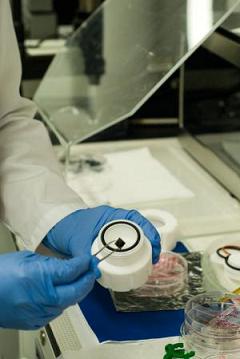
Alberta | Posted on November 18th, 2010Jillian Buriak is a senior researcher at the National Institute for Nanotechnology. One of her group's projects could further revolutionize the production of computer chips.
After a short stint in the microwave, a silicon chip prepared using plastic polymers forms a pattern of lines or rings that is far more complex than what a conventional computer chip has. The lines formed from this reaction, only tens of nanometers apart from each other, act as a template for conductive material to be applied on.
"The polymer can be induced with a little bit of outside intervention. [Polymers] can say, 'Hey, I'm going to form these rings.' They can do it perfectly," Buriak said.
The outside intervention, a simple microwave oven, was the U of A group's big innovation. To make a computer chip template that complex, it can take up to three days by normal industry methods. The industry set a goal of cutting this down to four minutes; the group found that a microwave could do it in 20 seconds.
Ken Harris, a researcher working under Buriak, came up with the original idea for this inexpensive and unconventional method, along with other members of the team.
"The fact that [the rings] assemble � people have known that for quite a while now [�] That, we didn't invent. But the technique for making that happen quickly is brand new."
Harris said the fact that there are even more lines than a conventional computer chips could have implications for electronics.
"The more devices you can pack onto a chip, the faster and more powerful that computer is. So a lot of that depends on how far [the lines] are separated."
The computer chip industry wants to find a way to produce chips with a high level of density as efficiently as possible. Since the scale is so small, the alignment of the pattern has to be perfect or else the chip becomes worthless. If it is possible to produce properly aligned chips with equipment as inexpensive as a household microwave, Buriak explained that it could have serious implications for the industry.
There are more applications for the process than mass-producing faster chips, according to Buriak. The relationship between the polymers that create the chip template is similar to how living cells recognize one another and form a larger entity. By treating these cells the same way, it may be possible to interface living cells with silicon the same way the plastic polymers work.
####
For more information, please click here
Copyright © University of Alberta
If you have a comment, please Contact us.Issuers of news releases, not 7th Wave, Inc. or Nanotechnology Now, are solely responsible for the accuracy of the content.
Bookmark:


| Related News Press |
News and information
![]() Quantum computer improves AI predictions April 17th, 2026
Quantum computer improves AI predictions April 17th, 2026
![]() Flexible sensor gains sensitivity under pressure April 17th, 2026
Flexible sensor gains sensitivity under pressure April 17th, 2026
![]() A reusable chip for particulate matter sensing April 17th, 2026
A reusable chip for particulate matter sensing April 17th, 2026
![]() Detecting vibrational quantum beating in the predissociation dynamics of SF6 using time-resolved photoelectron spectroscopy April 17th, 2026
Detecting vibrational quantum beating in the predissociation dynamics of SF6 using time-resolved photoelectron spectroscopy April 17th, 2026
Possible Futures
![]() A fundamentally new therapeutic approach to cystic fibrosis: Nanobody repairs cellular defect April 17th, 2026
A fundamentally new therapeutic approach to cystic fibrosis: Nanobody repairs cellular defect April 17th, 2026
![]() UC Irvine physicists discover method to reverse �quantum scrambling� : The work addresses the problem of information loss in quantum computing system April 17th, 2026
UC Irvine physicists discover method to reverse �quantum scrambling� : The work addresses the problem of information loss in quantum computing system April 17th, 2026
Academic/Education
![]() Rice University launches Rice Synthetic Biology Institute to improve lives January 12th, 2024
Rice University launches Rice Synthetic Biology Institute to improve lives January 12th, 2024
![]() Multi-institution, $4.6 million NSF grant to fund nanotechnology training September 9th, 2022
Multi-institution, $4.6 million NSF grant to fund nanotechnology training September 9th, 2022
Chip Technology
![]() A reusable chip for particulate matter sensing April 17th, 2026
A reusable chip for particulate matter sensing April 17th, 2026
![]() Metasurfaces smooth light to boost magnetic sensing precision January 30th, 2026
Metasurfaces smooth light to boost magnetic sensing precision January 30th, 2026
Nanoelectronics
![]() Lab to industry: InSe wafer-scale breakthrough for future electronics August 8th, 2025
Lab to industry: InSe wafer-scale breakthrough for future electronics August 8th, 2025
![]() Interdisciplinary: Rice team tackles the future of semiconductors Multiferroics could be the key to ultralow-energy computing October 6th, 2023
Interdisciplinary: Rice team tackles the future of semiconductors Multiferroics could be the key to ultralow-energy computing October 6th, 2023
![]() Key element for a scalable quantum computer: Physicists from Forschungszentrum J�lich and RWTH Aachen University demonstrate electron transport on a quantum chip September 23rd, 2022
Key element for a scalable quantum computer: Physicists from Forschungszentrum J�lich and RWTH Aachen University demonstrate electron transport on a quantum chip September 23rd, 2022
![]() Reduced power consumption in semiconductor devices September 23rd, 2022
Reduced power consumption in semiconductor devices September 23rd, 2022
|
|
||
|
|
||
| The latest news from around the world, FREE | ||
|
|
||
|
|
||
| Premium Products | ||
|
|
||
|
Only the news you want to read!
Learn More |
||
|
|
||
|
Full-service, expert consulting
Learn More |
||
|
|
||