Home > Press > The Nano World of Shrinky Dinks
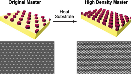 |
| One programmable soft lithography recipe: (1) Start with a thermoplastic substrate. (2) Perform SANE. (3) Heat substrate. (4) Create different nanopatterns with same feature sizes. (5) Repeat. |
Abstract:
Low-cost nanopatterning method utilizes popular shrinkable plastic
The Nano World of Shrinky Dinks
Evanston, IL | Posted on August 16th, 2010The magical world of Shrinky Dinks -- an arts and crafts material used by children since the 1970s -- has taken up residence in a Northwestern University laboratory. A team of nanoscientists is using the flexible plastic sheets as the backbone of a new inexpensive way to create, test and mass-produce large-area patterns on the nanoscale.
"Anyone needing access to large-area nanoscale patterns on the cheap could benefit from this method," said Teri W. Odom, associate professor of chemistry and Dow Chemical Company Research Professor in the Weinberg College of Arts and Sciences. Odom led the research. "It is a simple, low-cost and high-throughput nanopatterning method that can be done in any laboratory."
Details of the solvent-assisted nanoscale embossing (SANE) method are published by the journal Nano Letters. The work also will appear as the cover story of the journal's February 2011 issue.
The method offers unprecedented opportunities to manipulate the electronic, photonic and magnetic properties of nanomaterials. It also easily controls a pattern's size and symmetry and can be used to produce millions of copies of the pattern over a large area. Potential applications include devices that take advantage of nanoscale patterns, such as solar cells, high-density displays, computers and chemical and biological sensors.
"No other existing nanopatterning method can both prototype arbitrary patterns with small separations and reproduce them over six-inch wafers for less than $100," Odom said.
Starting with a single master pattern, the simple yet potentially transformative method can be used to create new nanoscale masters with variable spacings and feature sizes. SANE can increase the spacing of patterns up to 100 percent as well as decrease them down to 50 percent in a single step, merely by stretching or heating (shrinking) the polymer substrate (the Shrinky Dinks material). Also, SANE can reduce critical feature sizes as small as 45 percent compared to the master by controlled swelling of patterned polymer molds with different solvents. SANE works from the nanoscale to the macroscale.
Biologists, chemists and physicists who are not familiar with nanopatterning now can use SANE for research at the nanoscale. Those working on solar energy, data storage and plasmonics will find the method particularly useful, Odom said.
For example, in a plasmonics application, Odom and her research team used the patterning capabilities to generate metal nanoparticle arrays with continuously variable separations on the same substrate.
SANE offers a way to meet three grand challenges in nanofabrication from the same -- and a single -- master pattern: (1) creating programmable array densities, (2) reducing critical feature sizes, and (3) designing different and reconfigurable lattice symmetries over large areas and in a massively parallel manner.
The National Science Foundation supported the research.
The title of the Nano Letters paper is "Programmable Soft Lithography: Solvent-Assisted Nanoscale Embossing." In addition to Odom, other authors of the paper are Min Hyung Lee, Mark D. Huntington, Wei Zhou and Jiun-Chan Yang, all from Northwestern.
####
For more information, please click here
Contacts:
Megan Fellman is the science and engineering editor.
Contact her at
Copyright © Northwestern University
If you have a comment, please Contact us.Issuers of news releases, not 7th Wave, Inc. or Nanotechnology Now, are solely responsible for the accuracy of the content.
Bookmark:


| Related News Press |
News and information
![]() Quantum computer improves AI predictions April 17th, 2026
Quantum computer improves AI predictions April 17th, 2026
![]() Flexible sensor gains sensitivity under pressure April 17th, 2026
Flexible sensor gains sensitivity under pressure April 17th, 2026
![]() A reusable chip for particulate matter sensing April 17th, 2026
A reusable chip for particulate matter sensing April 17th, 2026
![]() Detecting vibrational quantum beating in the predissociation dynamics of SF6 using time-resolved photoelectron spectroscopy April 17th, 2026
Detecting vibrational quantum beating in the predissociation dynamics of SF6 using time-resolved photoelectron spectroscopy April 17th, 2026
Display technology/LEDs/SS Lighting/OLEDs
![]() Spinel-type sulfide semiconductors to operate the next-generation LEDs and solar cells For solar-cell absorbers and green-LED source October 3rd, 2025
Spinel-type sulfide semiconductors to operate the next-generation LEDs and solar cells For solar-cell absorbers and green-LED source October 3rd, 2025
![]() Efficient and stable hybrid perovskite-organic light-emitting diodes with external quantum efficiency exceeding 40 per cent July 5th, 2024
Efficient and stable hybrid perovskite-organic light-emitting diodes with external quantum efficiency exceeding 40 per cent July 5th, 2024
Govt.-Legislation/Regulation/Funding/Policy
![]() Quantum computer improves AI predictions April 17th, 2026
Quantum computer improves AI predictions April 17th, 2026
![]() Metasurfaces smooth light to boost magnetic sensing precision January 30th, 2026
Metasurfaces smooth light to boost magnetic sensing precision January 30th, 2026
![]() New imaging approach transforms study of bacterial biofilms August 8th, 2025
New imaging approach transforms study of bacterial biofilms August 8th, 2025
Possible Futures
![]() A fundamentally new therapeutic approach to cystic fibrosis: Nanobody repairs cellular defect April 17th, 2026
A fundamentally new therapeutic approach to cystic fibrosis: Nanobody repairs cellular defect April 17th, 2026
![]() UC Irvine physicists discover method to reverse �quantum scrambling� : The work addresses the problem of information loss in quantum computing system April 17th, 2026
UC Irvine physicists discover method to reverse �quantum scrambling� : The work addresses the problem of information loss in quantum computing system April 17th, 2026
Academic/Education
![]() Rice University launches Rice Synthetic Biology Institute to improve lives January 12th, 2024
Rice University launches Rice Synthetic Biology Institute to improve lives January 12th, 2024
![]() Multi-institution, $4.6 million NSF grant to fund nanotechnology training September 9th, 2022
Multi-institution, $4.6 million NSF grant to fund nanotechnology training September 9th, 2022
Sensors
![]() Flexible sensor gains sensitivity under pressure April 17th, 2026
Flexible sensor gains sensitivity under pressure April 17th, 2026
![]() Tiny nanosheets, big leap: A new sensor detects ethanol at ultra-low levels January 30th, 2026
Tiny nanosheets, big leap: A new sensor detects ethanol at ultra-low levels January 30th, 2026
![]() From sensors to smart systems: the rise of AI-driven photonic noses January 30th, 2026
From sensors to smart systems: the rise of AI-driven photonic noses January 30th, 2026
![]() Sensors innovations for smart lithium-based batteries: advancements, opportunities, and potential challenges August 8th, 2025
Sensors innovations for smart lithium-based batteries: advancements, opportunities, and potential challenges August 8th, 2025
Nanoelectronics
![]() Lab to industry: InSe wafer-scale breakthrough for future electronics August 8th, 2025
Lab to industry: InSe wafer-scale breakthrough for future electronics August 8th, 2025
![]() Interdisciplinary: Rice team tackles the future of semiconductors Multiferroics could be the key to ultralow-energy computing October 6th, 2023
Interdisciplinary: Rice team tackles the future of semiconductors Multiferroics could be the key to ultralow-energy computing October 6th, 2023
![]() Key element for a scalable quantum computer: Physicists from Forschungszentrum J�lich and RWTH Aachen University demonstrate electron transport on a quantum chip September 23rd, 2022
Key element for a scalable quantum computer: Physicists from Forschungszentrum J�lich and RWTH Aachen University demonstrate electron transport on a quantum chip September 23rd, 2022
![]() Reduced power consumption in semiconductor devices September 23rd, 2022
Reduced power consumption in semiconductor devices September 23rd, 2022
Announcements
![]() A fundamentally new therapeutic approach to cystic fibrosis: Nanobody repairs cellular defect April 17th, 2026
A fundamentally new therapeutic approach to cystic fibrosis: Nanobody repairs cellular defect April 17th, 2026
![]() UC Irvine physicists discover method to reverse �quantum scrambling� : The work addresses the problem of information loss in quantum computing system April 17th, 2026
UC Irvine physicists discover method to reverse �quantum scrambling� : The work addresses the problem of information loss in quantum computing system April 17th, 2026
Photonics/Optics/Lasers
![]() Metasurfaces smooth light to boost magnetic sensing precision January 30th, 2026
Metasurfaces smooth light to boost magnetic sensing precision January 30th, 2026
![]() From sensors to smart systems: the rise of AI-driven photonic noses January 30th, 2026
From sensors to smart systems: the rise of AI-driven photonic noses January 30th, 2026
Solar/Photovoltaic
![]() Spinel-type sulfide semiconductors to operate the next-generation LEDs and solar cells For solar-cell absorbers and green-LED source October 3rd, 2025
Spinel-type sulfide semiconductors to operate the next-generation LEDs and solar cells For solar-cell absorbers and green-LED source October 3rd, 2025
![]() KAIST researchers introduce new and improved, next-generation perovskite solar cell November 8th, 2024
KAIST researchers introduce new and improved, next-generation perovskite solar cell November 8th, 2024
![]() Groundbreaking precision in single-molecule optoelectronics August 16th, 2024
Groundbreaking precision in single-molecule optoelectronics August 16th, 2024
![]() Development of zinc oxide nanopagoda array photoelectrode: photoelectrochemical water-splitting hydrogen production January 12th, 2024
Development of zinc oxide nanopagoda array photoelectrode: photoelectrochemical water-splitting hydrogen production January 12th, 2024
|
|
||
|
|
||
| The latest news from around the world, FREE | ||
|
|
||
|
|
||
| Premium Products | ||
|
|
||
|
Only the news you want to read!
Learn More |
||
|
|
||
|
Full-service, expert consulting
Learn More |
||
|
|
||