Home > Press > Electron orbits in multilayer graphene find energy gaps
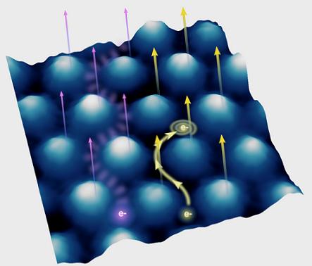 |
| Graphene Electron Motion |
Abstract:
Researchers have taken one more step toward understanding the unique and often unexpected properties of graphene, a two-dimensional carbon material that has attracted interest because of its potential applications in future generations of electronic devices.
By John Toon
Electron orbits in multilayer graphene find energy gaps
Atlanta, GA | Posted on August 10th, 2010In the Aug. 8 advance online edition of the journal Nature Physics, researchers from the Georgia Institute of Technology and the National Institute of Standards and Technology (NIST) describe for the first time how the orbits of electrons are distributed spatially by magnetic fields applied to layers of epitaxial graphene.
The research team also found that these electron orbits can interact with the substrate on which the graphene is grown, creating energy gaps that affect how electron waves move through the multilayer material. These energy gaps could have implications for the designers of certain graphene-based electronic devices.
"The regular pattern of energy gaps in the graphene surface creates regions where electron transport is not allowed," said Phillip N. First, a professor in the Georgia Tech School of Physics and one of the paper's co-authors. "Electron waves would have to go around these regions, requiring new patterns of electron wave interference. Understanding such interference will be important for bi-layer graphene devices that have been proposed, and may be important for other lattice-matched substrates used to support graphene and graphene devices."
In a magnetic field, an electron moves in a circular trajectory -- known as a cyclotron orbit -- whose radius depends on the size of the magnetic field and the energy of electron. For a constant magnetic field, that's a little like rolling a marble around in a large bowl, First said.
"At high energy, the marble orbits high in the bowl, while for lower energies, the orbit size is smaller and lower in the bowl," he explained. "The cyclotron orbits in graphene also depend on the electron energy and the local electron potential -- corresponding to the bowl -- but until now, the orbits hadn't been imaged directly."
Placed in a magnetic field, these orbits normally drift along lines of nearly constant electric potential. But when a graphene sample has small fluctuations in the potential, these "drift states" can become trapped at a hill or valley in the material that has closed constant potential contours. Such trapping of charge carriers is important for the quantum Hall effect, in which precisely quantized resistance results from charge conduction solely through the orbits that skip along the edges of the material.
The study focused on one particular electron orbit: a zero-energy orbit that is unique to graphene. Because electrons are matter waves, interference within a material affects how their energy relates to the velocity of the wave -- and reflected waves added to an incoming wave can combine to produce a slower composite wave. Electrons moving through the unique "chicken-wire" arrangement of carbon-carbon bonds in the graphene interfere in a way that leaves the wave velocity the same for all energy levels.
In addition to finding that energy states follow contours of constant electric potential, the researchers discovered specific areas on the graphene surface where the orbital energy of the electrons changes from one atom to the next. That creates an energy gap within isolated patches on the surface.
"By examining their distribution over the surface for different magnetic fields, we determined that the energy gap is due to a subtle interaction with the substrate, which consists of multilayer graphene grown on a silicon carbide wafer," First explained.
In multilayer epitaxial graphene, each layer's symmetrical sublattice is rotated slightly with respect to the next. In prior studies, researchers found that the rotations served to decouple the electronic properties of each graphene layer.
"Our findings hold the first indications of a small position-dependent interaction between the layers," said David L. Miller, the paper's first author and a graduate student in First's laboratory. "This interaction occurs only when the size of a cyclotron orbit -- which shrinks as the magnetic field is increased -- becomes smaller than the size of the observed patches."
The origin of the position dependent interaction is believed to be the "moir� pattern" of atomic alignments between two adjacent layers of graphene. In some regions, atoms of one layer lie atop atoms of the layer below, while in other regions, none of the atoms align with the atoms in the layer below. In still other regions, half of the atoms have neighbors in the underlayer, an instance in which the symmetry of the carbon atoms is broken and the Landau level -- discrete energy level of the electrons -- splits into two different energies.
Experimentally, the researchers examined a sample of epitaxial graphene grown at Georgia Tech in the laboratory of Professor Walt de Heer, using techniques developed by his research team over the past several years.
They used the tip of a custom-built scanning-tunneling microscope (STM) to probe the atomic-scale electronic structure of the graphene in a technique known as scanning tunneling spectroscopy. The tip was moved across the surface of a 100-square nanometer section of graphene, and spectroscopic data was acquired every 0.4 nanometers.
The measurements were done at 4.3 degrees Kelvin to take advantage of the fact that energy resolution is proportional to the temperature. The scanning-tunneling microscope, designed and built by Joseph Stroscio at NIST's Center for Nanoscale Science and Technology, used a superconducting magnet to provide the magnetic fields needed to study the orbits.
According to First, the study raises a number of questions for future research, including how the energy gaps will affect electron transport properties, how the observed effects may impact proposed bi-layer graphene coherent devices -- and whether the new phenomenon can be controlled.
"This study is really a stepping stone in long path to understanding the subtleties of graphene's interesting properties," he said. "This material is different from anything we have worked with before in electronics."
In addition to those already mentioned, the study also included Walt de Heer, Kevin D. Kubista, Ming Ruan, and Markus Kinderman from Georgia Tech and Gregory M. Rutter from NIST. The research was supported by the National Science Foundation, the Semiconductor Research Corporation and the W.M. Keck Foundation. Additional assistance was provided by Georgia Tech's Materials Research Science and Engineering Center (MRSEC).
####
For more information, please click here
Contacts:
Media Relations Contacts:
John Toon
404-894-6986
Abby Vogel Robinson
404-385-3364
Copyright © Georgia Institute of Technology
If you have a comment, please Contact us.Issuers of news releases, not 7th Wave, Inc. or Nanotechnology Now, are solely responsible for the accuracy of the content.
Bookmark:


| Related News Press |
News and information
![]() Quantum computer improves AI predictions April 17th, 2026
Quantum computer improves AI predictions April 17th, 2026
![]() Flexible sensor gains sensitivity under pressure April 17th, 2026
Flexible sensor gains sensitivity under pressure April 17th, 2026
![]() A reusable chip for particulate matter sensing April 17th, 2026
A reusable chip for particulate matter sensing April 17th, 2026
![]() Detecting vibrational quantum beating in the predissociation dynamics of SF6 using time-resolved photoelectron spectroscopy April 17th, 2026
Detecting vibrational quantum beating in the predissociation dynamics of SF6 using time-resolved photoelectron spectroscopy April 17th, 2026
Govt.-Legislation/Regulation/Funding/Policy
![]() Quantum computer improves AI predictions April 17th, 2026
Quantum computer improves AI predictions April 17th, 2026
![]() Metasurfaces smooth light to boost magnetic sensing precision January 30th, 2026
Metasurfaces smooth light to boost magnetic sensing precision January 30th, 2026
![]() New imaging approach transforms study of bacterial biofilms August 8th, 2025
New imaging approach transforms study of bacterial biofilms August 8th, 2025
Possible Futures
![]() A fundamentally new therapeutic approach to cystic fibrosis: Nanobody repairs cellular defect April 17th, 2026
A fundamentally new therapeutic approach to cystic fibrosis: Nanobody repairs cellular defect April 17th, 2026
![]() UC Irvine physicists discover method to reverse �quantum scrambling� : The work addresses the problem of information loss in quantum computing system April 17th, 2026
UC Irvine physicists discover method to reverse �quantum scrambling� : The work addresses the problem of information loss in quantum computing system April 17th, 2026
Academic/Education
![]() Rice University launches Rice Synthetic Biology Institute to improve lives January 12th, 2024
Rice University launches Rice Synthetic Biology Institute to improve lives January 12th, 2024
![]() Multi-institution, $4.6 million NSF grant to fund nanotechnology training September 9th, 2022
Multi-institution, $4.6 million NSF grant to fund nanotechnology training September 9th, 2022
Nanotubes/Buckyballs/Fullerenes/Nanorods/Nanostrings/Nanosheets
![]() Tiny nanosheets, big leap: A new sensor detects ethanol at ultra-low levels January 30th, 2026
Tiny nanosheets, big leap: A new sensor detects ethanol at ultra-low levels January 30th, 2026
![]() Enhancing power factor of p- and n-type single-walled carbon nanotubes April 25th, 2025
Enhancing power factor of p- and n-type single-walled carbon nanotubes April 25th, 2025
![]() Chainmail-like material could be the future of armor: First 2D mechanically interlocked polymer exhibits exceptional flexibility and strength January 17th, 2025
Chainmail-like material could be the future of armor: First 2D mechanically interlocked polymer exhibits exceptional flexibility and strength January 17th, 2025
![]() Innovative biomimetic superhydrophobic coating combines repair and buffering properties for superior anti-erosion December 13th, 2024
Innovative biomimetic superhydrophobic coating combines repair and buffering properties for superior anti-erosion December 13th, 2024
Nanoelectronics
![]() Lab to industry: InSe wafer-scale breakthrough for future electronics August 8th, 2025
Lab to industry: InSe wafer-scale breakthrough for future electronics August 8th, 2025
![]() Interdisciplinary: Rice team tackles the future of semiconductors Multiferroics could be the key to ultralow-energy computing October 6th, 2023
Interdisciplinary: Rice team tackles the future of semiconductors Multiferroics could be the key to ultralow-energy computing October 6th, 2023
![]() Key element for a scalable quantum computer: Physicists from Forschungszentrum J�lich and RWTH Aachen University demonstrate electron transport on a quantum chip September 23rd, 2022
Key element for a scalable quantum computer: Physicists from Forschungszentrum J�lich and RWTH Aachen University demonstrate electron transport on a quantum chip September 23rd, 2022
![]() Reduced power consumption in semiconductor devices September 23rd, 2022
Reduced power consumption in semiconductor devices September 23rd, 2022
Announcements
![]() A fundamentally new therapeutic approach to cystic fibrosis: Nanobody repairs cellular defect April 17th, 2026
A fundamentally new therapeutic approach to cystic fibrosis: Nanobody repairs cellular defect April 17th, 2026
![]() UC Irvine physicists discover method to reverse �quantum scrambling� : The work addresses the problem of information loss in quantum computing system April 17th, 2026
UC Irvine physicists discover method to reverse �quantum scrambling� : The work addresses the problem of information loss in quantum computing system April 17th, 2026
Tools
![]() Metasurfaces smooth light to boost magnetic sensing precision January 30th, 2026
Metasurfaces smooth light to boost magnetic sensing precision January 30th, 2026
![]() From sensors to smart systems: the rise of AI-driven photonic noses January 30th, 2026
From sensors to smart systems: the rise of AI-driven photonic noses January 30th, 2026
![]() Japan launches fully domestically produced quantum computer: Expo visitors to experience quantum computing firsthand August 8th, 2025
Japan launches fully domestically produced quantum computer: Expo visitors to experience quantum computing firsthand August 8th, 2025
|
|
||
|
|
||
| The latest news from around the world, FREE | ||
|
|
||
|
|
||
| Premium Products | ||
|
|
||
|
Only the news you want to read!
Learn More |
||
|
|
||
|
Full-service, expert consulting
Learn More |
||
|
|
||