Home > Press > Intel Milestone Confirms Light Beams Can Replace Electronic Signals for Future Computers
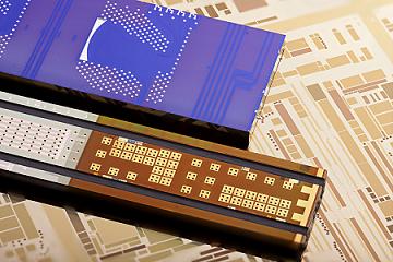 |
| The two silicon chips are at the heart of the 50G Silicon Photonics link. The lower chip is used to generate light and send data, while the upper chip is used to receive laser light and convert the optical information back into electrical 1s and 0s. |
Abstract:
Intel Creates World's First End-to-End Silicon Photonics Connection with Integrated Lasers; Could Revolutionize Computer Design, Dramatically Increase Performance, Save Energy
Intel Milestone Confirms Light Beams Can Replace Electronic Signals for Future Computers
Santa Clara, CA | Posted on July 29th, 2010Intel Corporation today announced an important advance in the quest to use light beams to replace the use of electrons to carry data in and around computers. The company has developed a research prototype representing the world's first silicon-based optical data connection with integrated lasers. The link can move data over longer distances and many times faster than today's copper technology; up to 50 gigabits of data per second. This is the equivalent of an entire HD movie being transmitted each second.
Today computer components are connected to each other using copper cables or traces on circuit boards. Due to the signal degradation that comes with using metals such as copper to transmit data, these cables have a limited maximum length. This limits the design of computers, forcing processors, memory and other components to be placed just inches from each other. Today's research achievement is another step toward replacing these connections with extremely thin and light optical fibers that can transfer much more data over far longer distances, radically changing the way computers of the future are designed and altering the way the datacenter of tomorrow is architected.
Silicon photonics will have applications across the computing industry. For example, at these data rates one could imagine a wall-sized 3D display for home entertainment and videoconferencing with a resolution so high that the actors or family members appear to be in the room with you. Tomorrow's datacenter or supercomputer may see components spread throughout a building or even an entire campus, communicating with each other at high speed, as opposed to being confined by heavy copper cables with limited capacity and reach. This will allow datacenter users, such as a search engine company, cloud computing provider or financial datacenter, to increase performance, capabilities and save significant costs in space and energy, or help scientists build more powerful supercomputers to solve the world's biggest problems.
Justin Rattner, Intel chief technology officer and director of Intel Labs, demonstrated the Silicon Photonics Link at the Integrated Photonics Research conference in Monterey, Calif. The 50Gbps link is akin to a "concept vehicle" that allows Intel researchers to test new ideas and continue the company's quest to develop technologies that transmit data over optical fibers, using light beams from low cost and easy to make silicon, instead of costly and hard to make devices using exotic materials like gallium arsenide. While telecommunications and other applications already use lasers to transmit information, current technologies are too expensive and bulky to be used for PC applications.
"This achievement of the world's first 50Gbps silicon photonics link with integrated hybrid silicon lasers marks a significant achievement in our long term vision of �siliconizing' photonics and bringing high bandwidth, low cost optical communications in and around future PCs, servers, and consumer devices" Rattner said.
The 50Gbps Silicon Photonics Link prototype is the result of a multi-year silicon photonics research agenda, which included numerous "world firsts." It is composed of a silicon transmitter and a receiver chip, each integrating all the necessary building blocks from previous Intel breakthroughs including the first Hybrid Silicon Laser co-developed with the University of California at Santa Barbara in 2006 as well as high-speed optical modulators and photodetectors announced in 2007.
The transmitter chip is composed of four such lasers, whose light beams each travel into an optical modulator that encodes data onto them at 12.5Gbps. The four beams are then combined and output to a single optical fiber for a total data rate of 50Gbps. At the other end of the link, the receiver chip separates the four optical beams and directs them into photo detectors, which convert data back into electrical signals. Both chips are assembled using low-cost manufacturing techniques familiar to the semiconductor industry. Intel researchers are already working to increase the data rate by scaling the modulator speed as well as increase the number of lasers per chip, providing a path to future terabit/s optical links - rates fast enough to transfer a copy of the entire contents of a typical laptop in one second.
This research is separate from Intel's Light Peak technology, though both are components of Intel's overall I/O strategy. Light Peak is an effort to bring a multi-protocol 10Gbps optical connection to Intel client platforms for nearer-term applications. Silicon Photonics research aims to use silicon integration to bring dramatic cost reductions, reach tera-scale data rates, and bring optical communications to an even broader set of high-volume applications. Today's achievement brings Intel a significant step closer to that goal.
(Video here: www.intel.com/pressroom/archive/releases/20100727comp_sm.htm)
####
About Intel
Intel (NASDAQ: INTC) is a world leader in computing innovation. The company designs and builds the essential technologies that serve as the foundation for the world�s computing devices. Additional information about Intel is available at www.intel.com/pressroom and blogs.intel.com.
Intel is a trademark of Intel Corporation in the United States and other countries.
* Other names and brands may be claimed as the property of others.
For more information, please click here
Copyright © Intel
If you have a comment, please Contact us.Issuers of news releases, not 7th Wave, Inc. or Nanotechnology Now, are solely responsible for the accuracy of the content.
Bookmark:


| Related News Press |
News and information
![]() Quantum computer improves AI predictions April 17th, 2026
Quantum computer improves AI predictions April 17th, 2026
![]() Flexible sensor gains sensitivity under pressure April 17th, 2026
Flexible sensor gains sensitivity under pressure April 17th, 2026
![]() A reusable chip for particulate matter sensing April 17th, 2026
A reusable chip for particulate matter sensing April 17th, 2026
![]() Detecting vibrational quantum beating in the predissociation dynamics of SF6 using time-resolved photoelectron spectroscopy April 17th, 2026
Detecting vibrational quantum beating in the predissociation dynamics of SF6 using time-resolved photoelectron spectroscopy April 17th, 2026
Possible Futures
![]() A fundamentally new therapeutic approach to cystic fibrosis: Nanobody repairs cellular defect April 17th, 2026
A fundamentally new therapeutic approach to cystic fibrosis: Nanobody repairs cellular defect April 17th, 2026
![]() UC Irvine physicists discover method to reverse �quantum scrambling� : The work addresses the problem of information loss in quantum computing system April 17th, 2026
UC Irvine physicists discover method to reverse �quantum scrambling� : The work addresses the problem of information loss in quantum computing system April 17th, 2026
Chip Technology
![]() A reusable chip for particulate matter sensing April 17th, 2026
A reusable chip for particulate matter sensing April 17th, 2026
![]() Metasurfaces smooth light to boost magnetic sensing precision January 30th, 2026
Metasurfaces smooth light to boost magnetic sensing precision January 30th, 2026
Nanoelectronics
![]() Lab to industry: InSe wafer-scale breakthrough for future electronics August 8th, 2025
Lab to industry: InSe wafer-scale breakthrough for future electronics August 8th, 2025
![]() Interdisciplinary: Rice team tackles the future of semiconductors Multiferroics could be the key to ultralow-energy computing October 6th, 2023
Interdisciplinary: Rice team tackles the future of semiconductors Multiferroics could be the key to ultralow-energy computing October 6th, 2023
![]() Key element for a scalable quantum computer: Physicists from Forschungszentrum J�lich and RWTH Aachen University demonstrate electron transport on a quantum chip September 23rd, 2022
Key element for a scalable quantum computer: Physicists from Forschungszentrum J�lich and RWTH Aachen University demonstrate electron transport on a quantum chip September 23rd, 2022
![]() Reduced power consumption in semiconductor devices September 23rd, 2022
Reduced power consumption in semiconductor devices September 23rd, 2022
Announcements
![]() A fundamentally new therapeutic approach to cystic fibrosis: Nanobody repairs cellular defect April 17th, 2026
A fundamentally new therapeutic approach to cystic fibrosis: Nanobody repairs cellular defect April 17th, 2026
![]() UC Irvine physicists discover method to reverse �quantum scrambling� : The work addresses the problem of information loss in quantum computing system April 17th, 2026
UC Irvine physicists discover method to reverse �quantum scrambling� : The work addresses the problem of information loss in quantum computing system April 17th, 2026
Photonics/Optics/Lasers
![]() Metasurfaces smooth light to boost magnetic sensing precision January 30th, 2026
Metasurfaces smooth light to boost magnetic sensing precision January 30th, 2026
![]() From sensors to smart systems: the rise of AI-driven photonic noses January 30th, 2026
From sensors to smart systems: the rise of AI-driven photonic noses January 30th, 2026
|
|
||
|
|
||
| The latest news from around the world, FREE | ||
|
|
||
|
|
||
| Premium Products | ||
|
|
||
|
Only the news you want to read!
Learn More |
||
|
|
||
|
Full-service, expert consulting
Learn More |
||
|
|
||