Home > Press > AquiVia Fill Sets New Standards for Metallization Process Of the Most Advanced Through-Silicon Vias
 |
Abstract:
New Alchimer Fill Technology Supports Narrow, High-Aspect-Ratio TSVs,
Offering Real Estate Savings, Reduced Fill Time and Higher Reliability
AquiVia Fill Sets New Standards for Metallization Process Of the Most Advanced Through-Silicon Vias
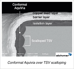
Paris | Posted on June 22nd, 2010Alchimer S.A., a leading provider of technology for the deposition of nanometric films used in both semiconductor interconnects and 3D through-silicon vias (TSV), today announced a groundbreaking advance for filling narrow, high-aspect-ratio TSVs while significantly reducing the need for chemical components in the metallization process.
The new AquiVia Fill process is an innovative, high-purity copper-plating chemistry that was specially developed to fill narrow TSVs with diameters of less than five microns and aspect ratios greater than 10:1. Reduced via diameter frees up substantial space on stacked chips, and improves signal integrity, where traditional manufacturing technologies have struggled to provide quality filling at an affordable cost.
"AquiVia Fill overcomes processing limitations in the current marketplace; lack of fill technology has been an obstacle to chip and system designers who are trying to pack as much power as possible into next-generation portable systems," said Dr. Claudio Truzzi, Alchimer's chief technology officer. "This new approach to via filling complements Alchimer's AquiVia XS seedless TSV films process, which deposits insulation and barrier layers in high aspect ratio TSVs prior to filling."
The combination of AquiVia XS and AquiVia Fill also extends designers' and chipmakers' ability to shorten the metallization process, and slashes overall cost of ownership compared to traditional electroplating metallization processes.
In contrast with current solutions based on strongly acidic, complex chemistries, AquiVia Fill is a mild basic solution that does not attack or degrade the underlying barrier or seed layer. It eliminates the need to electrically polarize the cathode before the introduction of the wafer. This procedure, called "hot entry", has historically been introduced to limit the acidic attack of the solution, but it seriously degrades the metallic films and is difficult to control.
In another distinct improvement over current solutions, AquiVia Fill contains no chlorine (Cl) components. Cl must be added to acidic solutions to boost the effect of accelerator and suppressor additives. As an added benefit, AquiVia Fill does not form CuCl crust on the anode, eliminating the risk of having crust fragments detach and deposit onto the wafer. This risk is so high in legacy solutions that a filtering membrane must be introduced between the wafer and the anode, significantly adding to the cost of the deposition equipment.
"The most distinct benefit of AquiVia Fill probably is its extremely low number of added components, improving the purity level of the plated copper and drastically reducing the risk of via pull-up during subsequent thermal cycles," Truzzi said. "This is typically due to previously deposited components bubbling up to the TSV's exposed surface."
Alchimer will start sampling AquiVia Fill with select customers by July 1.
####
About Alchimer
Founded in 2001 as a spin-off from the Commissariat � l�Energie Atomique, Alchimer is headquartered in Massy, France, near Paris.
Alchimer is backed by world class investors and staffed with a well-respected team of scientists who excel in the areas of surface science, chemistry, electrochemistry, physics, materials science and semiconductors, and who are second to none.
Recent awards include the prestigious R&D100, Red Herring 100 winner, Best of West 2008 and Best of West finalist in 2009.
For more information, please click here
Contacts:
Jana Yuen
Phone: +33158185930
Copyright © Alchimer
If you have a comment, please Contact us.Issuers of news releases, not 7th Wave, Inc. or Nanotechnology Now, are solely responsible for the accuracy of the content.
Bookmark:


| Related News Press |
News and information
![]() Quantum computer improves AI predictions April 17th, 2026
Quantum computer improves AI predictions April 17th, 2026
![]() Flexible sensor gains sensitivity under pressure April 17th, 2026
Flexible sensor gains sensitivity under pressure April 17th, 2026
![]() A reusable chip for particulate matter sensing April 17th, 2026
A reusable chip for particulate matter sensing April 17th, 2026
![]() Detecting vibrational quantum beating in the predissociation dynamics of SF6 using time-resolved photoelectron spectroscopy April 17th, 2026
Detecting vibrational quantum beating in the predissociation dynamics of SF6 using time-resolved photoelectron spectroscopy April 17th, 2026
Chip Technology
![]() A reusable chip for particulate matter sensing April 17th, 2026
A reusable chip for particulate matter sensing April 17th, 2026
![]() Metasurfaces smooth light to boost magnetic sensing precision January 30th, 2026
Metasurfaces smooth light to boost magnetic sensing precision January 30th, 2026
Nanoelectronics
![]() Lab to industry: InSe wafer-scale breakthrough for future electronics August 8th, 2025
Lab to industry: InSe wafer-scale breakthrough for future electronics August 8th, 2025
![]() Interdisciplinary: Rice team tackles the future of semiconductors Multiferroics could be the key to ultralow-energy computing October 6th, 2023
Interdisciplinary: Rice team tackles the future of semiconductors Multiferroics could be the key to ultralow-energy computing October 6th, 2023
![]() Key element for a scalable quantum computer: Physicists from Forschungszentrum J�lich and RWTH Aachen University demonstrate electron transport on a quantum chip September 23rd, 2022
Key element for a scalable quantum computer: Physicists from Forschungszentrum J�lich and RWTH Aachen University demonstrate electron transport on a quantum chip September 23rd, 2022
![]() Reduced power consumption in semiconductor devices September 23rd, 2022
Reduced power consumption in semiconductor devices September 23rd, 2022
Announcements
![]() A fundamentally new therapeutic approach to cystic fibrosis: Nanobody repairs cellular defect April 17th, 2026
A fundamentally new therapeutic approach to cystic fibrosis: Nanobody repairs cellular defect April 17th, 2026
![]() UC Irvine physicists discover method to reverse �quantum scrambling� : The work addresses the problem of information loss in quantum computing system April 17th, 2026
UC Irvine physicists discover method to reverse �quantum scrambling� : The work addresses the problem of information loss in quantum computing system April 17th, 2026
|
|
||
|
|
||
| The latest news from around the world, FREE | ||
|
|
||
|
|
||
| Premium Products | ||
|
|
||
|
Only the news you want to read!
Learn More |
||
|
|
||
|
Full-service, expert consulting
Learn More |
||
|
|
||