Home > Press > UC San Diego Engineers Demonstrate Smallest Laser to Operate at Room Temperature
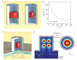 |
| Optimized metallo-dielectric laser cavity |
Abstract:
Imagine packing 4 billion nanolasers on a three-inch semiconductor wafer. That is now nearer to reality, thanks to researchers at the University of California, San Diego's Jacobs School of Engineering, who have demonstrated a micron-sized laser - less than one-thousandth of a millimeter on each side - that can operate at room temperature.
By Doug Ramsey
UC San Diego Engineers Demonstrate Smallest Laser to Operate at Room Temperature
San Diego, CA | Posted on May 6th, 2010Until now, the only way to operate such a nanolaser was to cool it cryogenically to offset the various losses in the device. The UCSD solution, as published online in advance of appearing in the May issue of the journal Nature Photonics, was to add super-thin layers of silica (glass) and aluminum to encase the core of each device.
"Shrinking the size of lasers to below their wavelength of emission has been challenging historically," said Yeshaiahu (Shaya) Fainman, principal investigator on the project and a Cymer professor in UC San Diego's Electrical and Computer Engineering (ECE) department. "What we have developed is a laser measuring one micron or less in all three dimensions - height, width and depth - that emits a beam with a wavelength of approximately 1.4 microns. These devices are truly �subwavelength,' because they are smaller than the wavelength of light they emit into air."
In theory these nanolasers could be packed densely on a wafer because the metallic aluminum layer helps to avoid coupling between neighboring nanolasers and also helps to conduct and dissipate the heat generated in the lasing process. "Using the aluminum shield gives the device superior heatsinking properties, which is important for device operation," added Fainman. "Using the metal shield confines the optical mode, so that two or more lasers can be placed very close to each other without interfering with each other's operation."
"Commercial applications of the technology are at least two years away," noted Maziar Nezhad, first author of the paper and an assistant project scientist in UC San Diego's ECE department. "But we also foresee its use in dense arrays of surface-emitting lasers for optical interconnects. The process could also be applied to the design of lasers for imaging in the far infrared range of the spectrum, due to the improved optical properties of metals in the infrared range."
To achieve a subwavelength laser, Nezhad and his colleagues in Fainman's Ultrafast and Nanoscale Optics Group worked through a series of approaches to create an efficient subwavelength cavity. The conventional approach used in the past for this purpose had been to use a fully dielectric cavity, but it quickly became evident that in the subwavelength size regime this type of cavity would not lead to a working solution. The UCSD team decided to incorporate a metal/dielectric composite layer in the nanolaser design to create an efficient resonant cavity and also to electromagnetically isolate the nanolaser from surrounding devices. The immediate candidates for the metal to be used - aluminum, gold and silver - all have good optical properties because they are very reflective (i.e., they absorb less light). In the tests described in the Nature Photonics article, aluminum was used, but Nezhad says that in theory, silver should be the most efficient shield.
The fabrication was done in the Nano3 clean room facility of the California Institute for Telecommunications and Information Technology (Calit2) at UC San Diego. To create and characterize the tiny lasers with their composite layers of glass and aluminum, the team made extensive use of Nano3's electron beam lithography, etchers, deposition tools, scanning electron microsocopy and optical profiling equipment. Once the wafers of micron-sized laser cavities were complete, optical measurements were performed in Fainman's lab in the Jacobs School of Engineering.
The researchers point out that it is of paramount importance to control the thickness of the glass layer. "If you don't put this glass layer around it, the metal would be too close to the optical field, and there would be too much interaction between the metal and the field and the cavity losses would be too high," explained Nezhad. "On the other hand, a glass layer that is too thick would result in a device that is either too large or has too little active semiconductor material -- reducing its efficacy. Through careful design, fabrication and testing, we found an optimal balance that created a room temperature laser that emits an infrared beam with a wavelength that is larger than the overall device dimensions."
Funding for the research came from the Defense Advanced Research Projects Agency (DARPA), with additional support from the National Science Foundation (NSF) and the Center for Integrated Access Networks (CIAN), an NSF-funded Engineering Research Center. Fainman is the Deputy Director of the nine-university collaboration.
The team at UC San Diego is one of seven around the country funded by DARPA through its Nanoscale Architectures for Coherent Hyper-Optic Sources (NACHOS) program. The program aims to create nanoscale lasers that "will enable close integration of photonic and electronic devices needed in emerging high-speed, processing-intense computing and communication platforms. In addition to reduced size, these lasers are expected to be power efficient and offer unprecedented modulation bandwidth. New capabilities, such as the ability to place large numbers of lasers on silicon chips, will be enabled by these devices."
While other NACHOS-funded teams were mainly working on solutions at cryogenic temperatures, UC San Diego focused on delivering an optically-pumped laser operating in pulse mode at room temperature - which it delivered last summer. In the ongoing Phase Two of the project, the research teams are working on replacing the optical pump with electrical pumping (also known as injection pumping) and by the end of the five-year program's final phase in 2012, the research teams are expected to demonstrate nanolasers operating in continuous rather than pulsed mode.
"With an optical pump, an external laser comes in at one wavelength and you excite the gain medium and then collect the light at the lasing wavelength. This requires a fairly large and complicated optical setup," explained Nezhad. "But if we can achieve these goals with an electrical pump, instead of relying on an external laser, you would only need a tiny power source to fuel the laser."
Looking ahead, principal investigator Shaya Fainman says the program at UC San Diego aims to accomplish DARPA's roadmap on time or ahead of schedule. "Making electrically pumped arrays of these lasers is one approach we are already working on, and we will also look at replacing aluminum with silver because of its unique optical properties," said the Calit2-affiliated scientist. "Another challenge will be to show that the properties of this micron-sized laser will hold up as we pack more and more lasers on a wafer."
Meanwhile, the teams at other universities are working on their own solutions to the challenges set forth by DARPA, so the researchers at UC San Diego won't be resting on their laurels.
Under principal investigator Shaya Fainman, the project team consisted of experts in optical and electromagnetic design, nanofabrication techniques, semiconductor materials and optical characterization. Nezhad worked on the optical design together with postdoctoral associate Amit Mizrahi, Boris Slutsky (a principal development engineer in Calit2) and ECE professor Vitaliy Lomakin. The team used electromagnetic wave theory and advanced finite element design tools to carry out the simulation and analysis of the nanolaser. Fainman and Nezhad also developed the fabrication process with another member of the NACHOS team, ECE professor Charles Tu. Graduate students Olesya Bondarenko and Liang Feng, together with Nezhad, put in long hours in Nano3 to fabricate the devices and in parallel, inside the photonics lab, grad student Aleksandar Simic and Nezhad handled the optical measurements and characterization of the nanolasers.
####
About UCSD
UC San Diego is dedicated to the advancement of knowledge through excellence in education and research at the undergraduate, graduate, professional school and postdoctoral levels. The campus is committed to community engagement, public service and industry partnerships in order to advance the health and well-being of our region, state, nation and the world. Our academic community of world-renowned faculty, bright students and dedicated staff is characterized by a culture of interdisciplinary collaboration and innovation which spans the globe.
To foster the best possible working and learning environment, our university strives to maintain a climate of fairness, cooperation, and professionalism, which is embodied in our campus Principles of Community. UC San Diego embraces diversity, equity, and inclusion as essential ingredients of academic excellence in higher education.
For more information, please click here
Contacts:
Media Contact:
Doug Ramsey
858-822-5825
Daniel Kane
858-534-3262
Copyright © UCSD
If you have a comment, please Contact us.Issuers of news releases, not 7th Wave, Inc. or Nanotechnology Now, are solely responsible for the accuracy of the content.
Bookmark:


| Related News Press |
News and information
![]() Quantum computer improves AI predictions April 17th, 2026
Quantum computer improves AI predictions April 17th, 2026
![]() Flexible sensor gains sensitivity under pressure April 17th, 2026
Flexible sensor gains sensitivity under pressure April 17th, 2026
![]() A reusable chip for particulate matter sensing April 17th, 2026
A reusable chip for particulate matter sensing April 17th, 2026
![]() Detecting vibrational quantum beating in the predissociation dynamics of SF6 using time-resolved photoelectron spectroscopy April 17th, 2026
Detecting vibrational quantum beating in the predissociation dynamics of SF6 using time-resolved photoelectron spectroscopy April 17th, 2026
Govt.-Legislation/Regulation/Funding/Policy
![]() Quantum computer improves AI predictions April 17th, 2026
Quantum computer improves AI predictions April 17th, 2026
![]() Metasurfaces smooth light to boost magnetic sensing precision January 30th, 2026
Metasurfaces smooth light to boost magnetic sensing precision January 30th, 2026
![]() New imaging approach transforms study of bacterial biofilms August 8th, 2025
New imaging approach transforms study of bacterial biofilms August 8th, 2025
Possible Futures
![]() A fundamentally new therapeutic approach to cystic fibrosis: Nanobody repairs cellular defect April 17th, 2026
A fundamentally new therapeutic approach to cystic fibrosis: Nanobody repairs cellular defect April 17th, 2026
![]() UC Irvine physicists discover method to reverse �quantum scrambling� : The work addresses the problem of information loss in quantum computing system April 17th, 2026
UC Irvine physicists discover method to reverse �quantum scrambling� : The work addresses the problem of information loss in quantum computing system April 17th, 2026
Academic/Education
![]() Rice University launches Rice Synthetic Biology Institute to improve lives January 12th, 2024
Rice University launches Rice Synthetic Biology Institute to improve lives January 12th, 2024
![]() Multi-institution, $4.6 million NSF grant to fund nanotechnology training September 9th, 2022
Multi-institution, $4.6 million NSF grant to fund nanotechnology training September 9th, 2022
Announcements
![]() A fundamentally new therapeutic approach to cystic fibrosis: Nanobody repairs cellular defect April 17th, 2026
A fundamentally new therapeutic approach to cystic fibrosis: Nanobody repairs cellular defect April 17th, 2026
![]() UC Irvine physicists discover method to reverse �quantum scrambling� : The work addresses the problem of information loss in quantum computing system April 17th, 2026
UC Irvine physicists discover method to reverse �quantum scrambling� : The work addresses the problem of information loss in quantum computing system April 17th, 2026
Tools
![]() Metasurfaces smooth light to boost magnetic sensing precision January 30th, 2026
Metasurfaces smooth light to boost magnetic sensing precision January 30th, 2026
![]() From sensors to smart systems: the rise of AI-driven photonic noses January 30th, 2026
From sensors to smart systems: the rise of AI-driven photonic noses January 30th, 2026
![]() Japan launches fully domestically produced quantum computer: Expo visitors to experience quantum computing firsthand August 8th, 2025
Japan launches fully domestically produced quantum computer: Expo visitors to experience quantum computing firsthand August 8th, 2025
Photonics/Optics/Lasers
![]() Metasurfaces smooth light to boost magnetic sensing precision January 30th, 2026
Metasurfaces smooth light to boost magnetic sensing precision January 30th, 2026
![]() From sensors to smart systems: the rise of AI-driven photonic noses January 30th, 2026
From sensors to smart systems: the rise of AI-driven photonic noses January 30th, 2026
Research partnerships
![]() Lab to industry: InSe wafer-scale breakthrough for future electronics August 8th, 2025
Lab to industry: InSe wafer-scale breakthrough for future electronics August 8th, 2025
![]() HKU physicists uncover hidden order in the quantum world through deconfined quantum critical points April 25th, 2025
HKU physicists uncover hidden order in the quantum world through deconfined quantum critical points April 25th, 2025
|
|
||
|
|
||
| The latest news from around the world, FREE | ||
|
|
||
|
|
||
| Premium Products | ||
|
|
||
|
Only the news you want to read!
Learn More |
||
|
|
||
|
Full-service, expert consulting
Learn More |
||
|
|
||