Home > Press > TAU combines new ionLiNE with Raith 150 for advanced nano-prototyping
 |
Abstract:
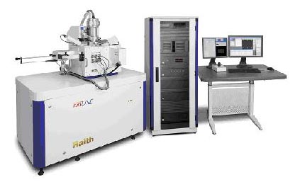
Raith GmbH, a leading provider of Nano-Structuring and Lithography systems, announced today the installation of a novel solution based on Raith's successful e-Line Electron Beam Lithography systems and their new Nano-FIB ion source and focused ion optics, at The Center for Nanoscience and Nanotechnology, Tel Aviv University, Israel. TAU will use the new ionLiNE - ion beam lithography system (IBL) to develop and extend its existing EBL facilities for advanced nano-prototyping applications.
TAU combines new ionLiNE with Raith 150 for advanced nano-prototyping
Dortmund, Germany | Posted on April 27th, 2010�EBL has been the benchmark for Nano-prototyping research for many years - combining speed with the established resist based nano-fabrication processing required for advanced research. By adding the complimentary technique of ion beam lithography, we will be able to extend the capabilities of our lithography process beyond the conventional limits, and investigate novel processes, giving higher levels of performance, both with and without the use of resist. The TAU Center for Nanoscience and Nanotechnology serves many collaborative partners within the University and external to it.
IBL is the natural compliment to EBL, adding automated three dimensional patterning, but while utilising all the standard design tools and layer patterning processes that are well understood for EBL. In addition to the delivery of one of the first ionLiNE IBL instruments, TAU and Raith have signed a joint development agreement to develop new IBL protocols for nano-prototyping applications for this emerging technique,' said Ori Cheshnovsky, head of the The Center for Nanoscience and Nanotechnology at TAU.
�This is the first time that applications which do not require ion beam imaging as the first step, such as small wafer level patterning, automated nanometer precision pattern placement and large area pattern stitching, which are effectively unknown within the conventional ion beam community, may be routinely performed. IBL solves these problems by applying true and tested, write field stitching capabilities, made possible by laser interferometer stage technology, to the versatile and direct write technique of ion beam patterning' said Lloyd Peto, Senior sales manager for ion beam lithography at Raith GmbH.
####
About Raith GmbH
Raith is an independent high technology enterprise, which, develops, sells and supports products to an international client base. The company has pioneered products for new markets, creating innovative solutions and enabling leading edge innovation in technology.
Raith offers complimentary solutions for nanolithography and fabrication with emphasis on R&D and small batch production for growing markets.
Raith is a partner for our customers within the academic community, semiconductor industry, microsystems technology and original equipment manufacturers(OEM).
About Tel Aviv University Center for Nanoscience and Nanotechnology
The TAU Center for Nanoscience and Nanotechnology (TAU-NST) was established in 2000 to support nano related research across four faculties (Exact Sciences, Engineering, Life Sciences and Medicine).
The centre provides the intellectual framework to catalyze interdisciplinary research, supported by the physical infrastructure, vital for nurturing leading-edge activities.
The central facility of the center encompasses state of the art equipment for construction, realization and general characterization of nano-structures. More than 50 researchers distributed in the above four faculties are affiliated with the center.
In addition to its primary research activities, the Center supports education programs in nanoscience, hosts visiting scientists, and promotes contacts and collaborations with granting agencies and with advanced technology industries.
For more information, please click here
Contacts:
Lloyd Peto
+44 7768 172049
Copyright © Raith GmbH
If you have a comment, please Contact us.Issuers of news releases, not 7th Wave, Inc. or Nanotechnology Now, are solely responsible for the accuracy of the content.
Bookmark:


| Related News Press |
News and information
![]() Simulating magnetization in a Heisenberg quantum spin chain April 5th, 2024
Simulating magnetization in a Heisenberg quantum spin chain April 5th, 2024
![]() NRL charters Navy�s quantum inertial navigation path to reduce drift April 5th, 2024
NRL charters Navy�s quantum inertial navigation path to reduce drift April 5th, 2024
![]() Discovery points path to flash-like memory for storing qubits: Rice find could hasten development of nonvolatile quantum memory April 5th, 2024
Discovery points path to flash-like memory for storing qubits: Rice find could hasten development of nonvolatile quantum memory April 5th, 2024
Academic/Education
![]() Rice University launches Rice Synthetic Biology Institute to improve lives January 12th, 2024
Rice University launches Rice Synthetic Biology Institute to improve lives January 12th, 2024
![]() Multi-institution, $4.6 million NSF grant to fund nanotechnology training September 9th, 2022
Multi-institution, $4.6 million NSF grant to fund nanotechnology training September 9th, 2022
Announcements
![]() NRL charters Navy�s quantum inertial navigation path to reduce drift April 5th, 2024
NRL charters Navy�s quantum inertial navigation path to reduce drift April 5th, 2024
![]() Discovery points path to flash-like memory for storing qubits: Rice find could hasten development of nonvolatile quantum memory April 5th, 2024
Discovery points path to flash-like memory for storing qubits: Rice find could hasten development of nonvolatile quantum memory April 5th, 2024
Tools
![]() Ferroelectrically modulate the Fermi level of graphene oxide to enhance SERS response November 3rd, 2023
Ferroelectrically modulate the Fermi level of graphene oxide to enhance SERS response November 3rd, 2023
![]() The USTC realizes In situ electron paramagnetic resonance spectroscopy using single nanodiamond sensors November 3rd, 2023
The USTC realizes In situ electron paramagnetic resonance spectroscopy using single nanodiamond sensors November 3rd, 2023
|
|
||
|
|
||
| The latest news from around the world, FREE | ||
|
|
||
|
|
||
| Premium Products | ||
|
|
||
|
Only the news you want to read!
Learn More |
||
|
|
||
|
Full-service, expert consulting
Learn More |
||
|
|
||