Home > Press > A Tiny Defect That May Create Smaller, Faster Electronics
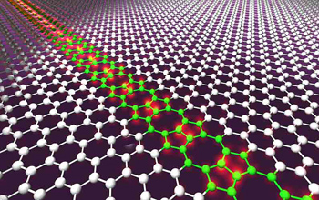 |
| An artist's conception of a row of intentional molecular defects in a sheet of graphene. The defects effectively create a metal wire in the sheet. This discovery may lead to smaller yet faster computers in the future. Credit: Y. Lin, USF |
Abstract:
Researchers at the University of South Florida have developed a technique to turn defects in graphene into tiny metallic wires
A Tiny Defect That May Create Smaller, Faster Electronics
Arlington, VA | Posted on April 1st, 2010When most of us hear the word 'defect', we think of a problem that has to be solved. But a team of researchers at the University of South Florida (USF) created a new defect that just might be a solution to a growing challenge in the development of future electronic devices.
The team lead by USF Professors Matthias Batzill and Ivan Oleynik, whose discovery was published yesterday in the journal Nature Nanotechnology, have developed a new method for adding an extended defect to graphene, a one-atom-thick planar sheet of carbon atoms that many believe could replace silicon as the material for building virtually all electronics.
It is not simple to work with graphene, however. To be useful in electronic applications like integrated circuits, small defects must be introduced to the material. Previous attempts at making the necessary defects have either proved inconsistent or produced samples in which only the edges of thin strips of graphene or graphene nanoribbons possessed a useful defect structure. However, atomically-sharp edges are difficult to create due to natural roughness and the uncontrolled chemistry of dangling bonds at the edge of the samples.
The USF team has now found a way to create a well-defined, extended defect several atoms across, containing octagonal and pentagonal carbon rings embedded in a perfect graphene sheet. This defect acts as a quasi-one-dimensional metallic wire that easily conducts electric current. Such defects could be used as metallic interconnects or elements of device structures of all-carbon, atomic-scale electronics.
So how did the team do it? The experimental group, guided by theory, used the self-organizing properties of a single-crystal nickel substrate, and used a metallic surface as a scaffold to synthesize two graphene half-sheets translated relative to each other with atomic precision. When the two halves merged at the boundary, they naturally formed an extended line defect. Both scanning tunneling microscopy and electronic structure calculations were used to confirm that this novel one-dimensional carbon defect possessed a well-defined, periodic atomic structure, as well as metallic properties within the narrow strip along the defect.
This tiny wire could have a big impact on the future of computer chips and the myriad of devices that use them. In the late 20th century, computer engineers described a phenomenon called Moore's Law, which holds that the number of transistors that can be affordably built into a computer processor doubles roughly every two years. This law has proven correct, and society has been reaping the benefits as computers become faster, smaller, and cheaper. In recent years, however, some physicists and engineers have come to believe that without new breakthroughs in new materials, we may soon reach the end of Moore's Law. As silicon-based transistors are brought down to their smallest possible scale, finding ways to pack more on a single processor becomes increasingly difficult.
Metallic wires in graphene may help to sustain the rate of microprocessor technology predicted by Moore's Law well into the future. The discovery by the USF team, with support from the National Science Foundation, may open the door to creation of the next generation of electronic devices using novel materials. Will this new discovery be available immediately in new nano-devices? Perhaps not right away, but it may provide a crucial step in the development of smaller, yet more powerful, electronic devices in the not-too-distant future.
Related Websites
Materials Simulation Lab at University of South Florida: msl.cas.usf.edu
Nanophysics and Surface Science Laboratory at USF: shell.cas.usf.edu/~mbatzill/
####
About National Science Foundation
The National Science Foundation (NSF) is an independent federal agency that supports fundamental research and education across all fields of science and engineering. In fiscal year (FY) 2010, its budget is about $6.9 billion. NSF funds reach all 50 states through grants to nearly 2,000 universities and institutions. Each year, NSF receives over 45,000 competitive requests for funding, and makes over 11,500 new funding awards. NSF also awards over $400 million in professional and service contracts yearly.
For more information, please click here
Contacts:
Media Contacts
Dana W. Cruikshank
NSF
(703) 292-7738
Copyright © National Science Foundation
If you have a comment, please Contact us.Issuers of news releases, not 7th Wave, Inc. or Nanotechnology Now, are solely responsible for the accuracy of the content.
Bookmark:


| Related News Press |
News and information
![]() Quantum computer improves AI predictions April 17th, 2026
Quantum computer improves AI predictions April 17th, 2026
![]() Flexible sensor gains sensitivity under pressure April 17th, 2026
Flexible sensor gains sensitivity under pressure April 17th, 2026
![]() A reusable chip for particulate matter sensing April 17th, 2026
A reusable chip for particulate matter sensing April 17th, 2026
![]() Detecting vibrational quantum beating in the predissociation dynamics of SF6 using time-resolved photoelectron spectroscopy April 17th, 2026
Detecting vibrational quantum beating in the predissociation dynamics of SF6 using time-resolved photoelectron spectroscopy April 17th, 2026
Possible Futures
![]() A fundamentally new therapeutic approach to cystic fibrosis: Nanobody repairs cellular defect April 17th, 2026
A fundamentally new therapeutic approach to cystic fibrosis: Nanobody repairs cellular defect April 17th, 2026
![]() UC Irvine physicists discover method to reverse �quantum scrambling� : The work addresses the problem of information loss in quantum computing system April 17th, 2026
UC Irvine physicists discover method to reverse �quantum scrambling� : The work addresses the problem of information loss in quantum computing system April 17th, 2026
Academic/Education
![]() Rice University launches Rice Synthetic Biology Institute to improve lives January 12th, 2024
Rice University launches Rice Synthetic Biology Institute to improve lives January 12th, 2024
![]() Multi-institution, $4.6 million NSF grant to fund nanotechnology training September 9th, 2022
Multi-institution, $4.6 million NSF grant to fund nanotechnology training September 9th, 2022
Chip Technology
![]() A reusable chip for particulate matter sensing April 17th, 2026
A reusable chip for particulate matter sensing April 17th, 2026
![]() Metasurfaces smooth light to boost magnetic sensing precision January 30th, 2026
Metasurfaces smooth light to boost magnetic sensing precision January 30th, 2026
Nanoelectronics
![]() Lab to industry: InSe wafer-scale breakthrough for future electronics August 8th, 2025
Lab to industry: InSe wafer-scale breakthrough for future electronics August 8th, 2025
![]() Interdisciplinary: Rice team tackles the future of semiconductors Multiferroics could be the key to ultralow-energy computing October 6th, 2023
Interdisciplinary: Rice team tackles the future of semiconductors Multiferroics could be the key to ultralow-energy computing October 6th, 2023
![]() Key element for a scalable quantum computer: Physicists from Forschungszentrum J�lich and RWTH Aachen University demonstrate electron transport on a quantum chip September 23rd, 2022
Key element for a scalable quantum computer: Physicists from Forschungszentrum J�lich and RWTH Aachen University demonstrate electron transport on a quantum chip September 23rd, 2022
![]() Reduced power consumption in semiconductor devices September 23rd, 2022
Reduced power consumption in semiconductor devices September 23rd, 2022
Discoveries
![]() Quantum computer improves AI predictions April 17th, 2026
Quantum computer improves AI predictions April 17th, 2026
![]() Flexible sensor gains sensitivity under pressure April 17th, 2026
Flexible sensor gains sensitivity under pressure April 17th, 2026
![]() A reusable chip for particulate matter sensing April 17th, 2026
A reusable chip for particulate matter sensing April 17th, 2026
![]() Detecting vibrational quantum beating in the predissociation dynamics of SF6 using time-resolved photoelectron spectroscopy April 17th, 2026
Detecting vibrational quantum beating in the predissociation dynamics of SF6 using time-resolved photoelectron spectroscopy April 17th, 2026
Announcements
![]() A fundamentally new therapeutic approach to cystic fibrosis: Nanobody repairs cellular defect April 17th, 2026
A fundamentally new therapeutic approach to cystic fibrosis: Nanobody repairs cellular defect April 17th, 2026
![]() UC Irvine physicists discover method to reverse �quantum scrambling� : The work addresses the problem of information loss in quantum computing system April 17th, 2026
UC Irvine physicists discover method to reverse �quantum scrambling� : The work addresses the problem of information loss in quantum computing system April 17th, 2026
|
|
||
|
|
||
| The latest news from around the world, FREE | ||
|
|
||
|
|
||
| Premium Products | ||
|
|
||
|
Only the news you want to read!
Learn More |
||
|
|
||
|
Full-service, expert consulting
Learn More |
||
|
|
||