Home > Press > Digging deep into diamonds
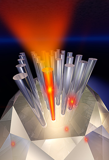 |
| Researchers used a top-down nanofabrication technique to embed color centers into a variety of machined structures. By creating large device arrays rather than just "one-of-a-kind" designs, the realization of quantum networks and systems, which require the integration and manipulation of many devices in parallel, is more likely. Illustration by Jay Penni. |
Abstract:
Diamond-based nanowire devices advance quantum science
Digging deep into diamonds
Cambridge, MA | Posted on February 15th, 2010By creating diamond-based nanowire devices, a team at Harvard University has taken another step toward making applications based on quantum science and technology possible.
The new device offers a bright, stable source of single photons at room temperature, an essential element in making fast and secure computing with light practical.
The finding could lead to a new class of nanostructured diamond devices suitable for quantum communication and computing, as well as advance areas ranging from biological and chemical sensing to scientific imaging.
Published in the Feb. 14 issue of Nature Nanotechnology, researchers led by Marko Loncar, assistant professor of electrical engineering at Harvard's School of Engineering and Applied Sciences (SEAS), found that the performance of a single photon source based on a light-emitting defect (color center) in a diamond could be improved by nanostructuring the diamond and embedding the defect within a diamond nanowire.
Scientists, in fact, first began exploiting the properties of natural diamonds after learning how to manipulate the electron spin, or intrinsic angular momentum, associated with the nitrogen vacancy (NV) color center of the gem. The quantum (qubit) state can be initialized and measured using light.
The color center "communicates" by emitting and absorbing photons. The flow of photons emitted from the color center provides a means to carry the resulting information, making the control, capture, and storage of photons essential for any kind of practical communication or computation. Gathering photons efficiently, however, is difficult since color centers are embedded deep inside the diamond.
"This presents a major problem if you want to interface a color center and integrate it into real-world applications," explains Loncar. "What was missing was an interface that connects the nano-world of a color center with the macro-world of optical fibers and lenses."
The diamond nanowire device offers a solution, providing a natural and efficient interface to probe an individual color center, making it brighter and increasing its sensitivity. The resulting enhanced optical properties increase photon collection by nearly a factor of ten relative to natural diamond devices.
"Our nanowire device can channel the photons that are emitted and direct them in a convenient way," says lead author Thomas Babinec, a graduate student at SEAS.
Further, the diamond nanowire is designed to overcome hurdles that have challenged other state-of-the-art systems � such as those based on fluorescent dye molecules, quantum dots, and carbon nanotubes � as the device can be readily replicated and integrated with a variety of nano-machined structures.
The researchers used a top-down nanofabrication technique to embed color centers into a variety of machined structures. By creating large device arrays rather than just "one-of-a-kind" designs, the realization of quantum networks and systems, which require the integration and manipulation of many devices in parallel, is more likely.
"We consider this an important step in enabling technology towards more practical optical systems based on this exciting material platform," says Loncar. "Starting with these synthetic, nanostructured diamond samples, we can start dreaming about the diamond-based devices and systems that could one day lead to applications in quantum science and technology as well as in sensing and imaging."
Loncar and Babinec's co-authors included research scholar Birgit Hausmann, graduate student Yinan Zhang, and postdoctoral student Mughees Khan, all at SEAS; graduate student Jero Maze in the Department of Physics at Harvard; and faculty member Phil R. Hemmer at Texas A&M University.
The researchers acknowledge the following support: Nanoscale Interdisciplinary Research Team (NIRT) grant from National Science Foundation (NSF), the NSF-funded Nanoscale Science and Engineering Center at Harvard (NSEC); the Defense Advanced Research Projects Agency (DARPA); and a National Defense Science and Engineering Graduate Fellowship and NSF Graduate Fellowship. All devices have been fabricated at the Center for Nanoscale Systems (CNS) at Harvard.
####
About Harvard University
Harvard University is made up of 11 principal academic units � ten faculties and the Radcliffe Institute for Advanced Study. The ten faculties oversee schools and divisions that offer courses and award academic degrees.
For more information, please click here
Copyright © Harvard University
If you have a comment, please Contact us.Issuers of news releases, not 7th Wave, Inc. or Nanotechnology Now, are solely responsible for the accuracy of the content.
Bookmark:


| Related News Press |
News and information
![]() Simulating magnetization in a Heisenberg quantum spin chain April 5th, 2024
Simulating magnetization in a Heisenberg quantum spin chain April 5th, 2024
![]() NRL charters Navy�s quantum inertial navigation path to reduce drift April 5th, 2024
NRL charters Navy�s quantum inertial navigation path to reduce drift April 5th, 2024
![]() Discovery points path to flash-like memory for storing qubits: Rice find could hasten development of nonvolatile quantum memory April 5th, 2024
Discovery points path to flash-like memory for storing qubits: Rice find could hasten development of nonvolatile quantum memory April 5th, 2024
Govt.-Legislation/Regulation/Funding/Policy
![]() NRL charters Navy�s quantum inertial navigation path to reduce drift April 5th, 2024
NRL charters Navy�s quantum inertial navigation path to reduce drift April 5th, 2024
![]() Discovery points path to flash-like memory for storing qubits: Rice find could hasten development of nonvolatile quantum memory April 5th, 2024
Discovery points path to flash-like memory for storing qubits: Rice find could hasten development of nonvolatile quantum memory April 5th, 2024
![]() Chemical reactions can scramble quantum information as well as black holes April 5th, 2024
Chemical reactions can scramble quantum information as well as black holes April 5th, 2024
Possible Futures
![]() Discovery points path to flash-like memory for storing qubits: Rice find could hasten development of nonvolatile quantum memory April 5th, 2024
Discovery points path to flash-like memory for storing qubits: Rice find could hasten development of nonvolatile quantum memory April 5th, 2024
![]() With VECSELs towards the quantum internet Fraunhofer: IAF achieves record output power with VECSEL for quantum frequency converters April 5th, 2024
With VECSELs towards the quantum internet Fraunhofer: IAF achieves record output power with VECSEL for quantum frequency converters April 5th, 2024
Nanotubes/Buckyballs/Fullerenes/Nanorods/Nanostrings
![]() Tests find no free-standing nanotubes released from tire tread wear September 8th, 2023
Tests find no free-standing nanotubes released from tire tread wear September 8th, 2023
![]() Detection of bacteria and viruses with fluorescent nanotubes July 21st, 2023
Detection of bacteria and viruses with fluorescent nanotubes July 21st, 2023
Quantum Computing
![]() Simulating magnetization in a Heisenberg quantum spin chain April 5th, 2024
Simulating magnetization in a Heisenberg quantum spin chain April 5th, 2024
![]() Discovery points path to flash-like memory for storing qubits: Rice find could hasten development of nonvolatile quantum memory April 5th, 2024
Discovery points path to flash-like memory for storing qubits: Rice find could hasten development of nonvolatile quantum memory April 5th, 2024
![]() With VECSELs towards the quantum internet Fraunhofer: IAF achieves record output power with VECSEL for quantum frequency converters April 5th, 2024
With VECSELs towards the quantum internet Fraunhofer: IAF achieves record output power with VECSEL for quantum frequency converters April 5th, 2024
![]() Chemical reactions can scramble quantum information as well as black holes April 5th, 2024
Chemical reactions can scramble quantum information as well as black holes April 5th, 2024
Sensors
Announcements
![]() NRL charters Navy�s quantum inertial navigation path to reduce drift April 5th, 2024
NRL charters Navy�s quantum inertial navigation path to reduce drift April 5th, 2024
![]() Discovery points path to flash-like memory for storing qubits: Rice find could hasten development of nonvolatile quantum memory April 5th, 2024
Discovery points path to flash-like memory for storing qubits: Rice find could hasten development of nonvolatile quantum memory April 5th, 2024
Quantum Dots/Rods
![]() A new kind of magnetism November 17th, 2023
A new kind of magnetism November 17th, 2023
![]() IOP Publishing celebrates World Quantum Day with the announcement of a special quantum collection and the winners of two prestigious quantum awards April 14th, 2023
IOP Publishing celebrates World Quantum Day with the announcement of a special quantum collection and the winners of two prestigious quantum awards April 14th, 2023
![]() Qubits on strong stimulants: Researchers find ways to improve the storage time of quantum information in a spin rich material January 27th, 2023
Qubits on strong stimulants: Researchers find ways to improve the storage time of quantum information in a spin rich material January 27th, 2023
![]() NIST�s grid of quantum islands could reveal secrets for powerful technologies November 18th, 2022
NIST�s grid of quantum islands could reveal secrets for powerful technologies November 18th, 2022
Alliances/Trade associations/Partnerships/Distributorships
![]() Chicago Quantum Exchange welcomes six new partners highlighting quantum technology solutions, from Chicago and beyond September 23rd, 2022
Chicago Quantum Exchange welcomes six new partners highlighting quantum technology solutions, from Chicago and beyond September 23rd, 2022
![]() University of Illinois Chicago joins Brookhaven Lab's Quantum Center June 10th, 2022
University of Illinois Chicago joins Brookhaven Lab's Quantum Center June 10th, 2022
Quantum nanoscience
![]() Simulating magnetization in a Heisenberg quantum spin chain April 5th, 2024
Simulating magnetization in a Heisenberg quantum spin chain April 5th, 2024
![]() Optically trapped quantum droplets of light can bind together to form macroscopic complexes March 8th, 2024
Optically trapped quantum droplets of light can bind together to form macroscopic complexes March 8th, 2024
![]() Bridging light and electrons January 12th, 2024
Bridging light and electrons January 12th, 2024
![]() 'Sudden death' of quantum fluctuations defies current theories of superconductivity: Study challenges the conventional wisdom of superconducting quantum transitions January 12th, 2024
'Sudden death' of quantum fluctuations defies current theories of superconductivity: Study challenges the conventional wisdom of superconducting quantum transitions January 12th, 2024
|
|
||
|
|
||
| The latest news from around the world, FREE | ||
|
|
||
|
|
||
| Premium Products | ||
|
|
||
|
Only the news you want to read!
Learn More |
||
|
|
||
|
Full-service, expert consulting
Learn More |
||
|
|
||