Home > Press > Nanoparticle assembly: Bridging spheres
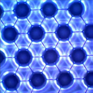 |
| Fig. 1: Micrograph view through the glass substrate showing the formation of a liquid bridge network during the evaporation of solvent. Reproduced from Ref. 1 � 2009 The American Chemical Society |
Abstract:
A lithographic approach based on evaporating solutions makes conducting networks of microwires for electronics
Nanoparticle assembly: Bridging spheres
Singapore | Posted on February 3rd, 2010A process to rival traditional lithography approaches, and which can be used to create microwire networks, is now a step closer to real applicability in future electronics. By optimizing the processing conditions for �evaporative lithography', a research team from Singapore and Australia has maximized the connectivity and conductivity of the microwire networks that conduct electricity1.
"Evaporative lithography could offer a cost-effective and environmentally friendly bench-top alternative to existing lithographic techniques such as photolithography, soft lithography and nanoimprinting," says team member Ivan Vakarelski from the A*STAR Institute of Chemical and Engineering Sciences, Singapore. He explains that the team is aiming primarily at creating large conducting microwire networks that, when deposited onto a glass substrate, could be used as transparent electrodes. These could be an alternative to the industry standard of indium tin oxide coatings, which would help circumvent the high cost and limited supply of indium.
Vakarelski and his co-workers created the microwire networks from solutions of gold nanoparticles of 20 nanometers diameter. As in their earlier work2, they first established a template of much larger latex microparticles on a substrate, then deposited solutions of the nanoparticles on top and allowed them to dry gradually. Surface tension then drove the solution into lines that formed �bridges' between neighboring latex particles (Fig. 1). Once the pattern was completely dry and the researchers removed the latex particles, the gold nanoparticles from the solution remained in a network of microwires.
The network pattern depends on the original positioning of the latex particles in the template, allowing different microwire designs to be easily realized. Vakarelski and his co-workers found that the networks can be improved for maximum conductivity and connectivity by adding a surfactant and treating the latex spheres with heat and oxygen plasma. They believe that these factors act to stabilize the latex spheres and the liquid bridges during drying to encourage full microwire networks to form.
Vakarelski is optimistic that the technique will progress to a level such that it will be used in manufacturing processes. He explains that this can be achieved by adapting the template production and expanding the size capacity to the scale of silicon wafers used in electronics.
The team's approach potentially has broader applications beyond electronics. "We can create special functional networks using semiconducting particles," Vakarelski says. Other examples include magnetic particles, carbon nanotubes, DNA, proteins and other macromolecules and even mixtures of these to create networks and nodes with desired properties.
The A*STAR affiliated authors in this highlight are from the Institute of Chemical and Engineering Sciences and the Institute of Materials Research and Engineering.
Reference
1. Vakarelski, I.U., Kwek, J.W., Tang, X.S., O'Shea, S.J. & Chan, D.Y.C. Particulate templates and ordered liquid bridge networks in evaporative lithography. Langmuir 25, 13311-13314 (2009).
2. Vakarelski, I.U., Chan, D.Y.C., Nonoguchi, T., Shinto, H. & Higashitani, K. Assembly of gold nanoparticles into microwire networks induced by drying liquid bridges. Physical Review Letters 102, 058303 (2009).
####
About A*STAR
A*STAR Research is an online and print publication highlighting some of the best research and technological developments at the research institutes of Singapore�s Agency for Science, Technology and Research (A*STAR). Established in 2002, A*STAR has thrived as a global research organization with a principal mission of fostering world-class scientific research and talent for a vibrant knowledge-based Singapore. A*STAR currently oversees 14 research institutes as well as 7 consortia and centers located in the Biopolis and Fusionopolis complexes and the vicinity, and supports extramural research in collaboration with universities, hospital research centers and other local and international partners. The various A*STAR institutes are involved in research in a wide range of scientific fields, coordinated and funded by Singapore�s Biomedical Research Council (BMRC) and Science and Engineering Research Council (SERC).
For more information, please click here
Copyright © A*STAR
If you have a comment, please Contact us.Issuers of news releases, not 7th Wave, Inc. or Nanotechnology Now, are solely responsible for the accuracy of the content.
Bookmark:


| Related News Press |
News and information
![]() Quantum computer improves AI predictions April 17th, 2026
Quantum computer improves AI predictions April 17th, 2026
![]() Flexible sensor gains sensitivity under pressure April 17th, 2026
Flexible sensor gains sensitivity under pressure April 17th, 2026
![]() A reusable chip for particulate matter sensing April 17th, 2026
A reusable chip for particulate matter sensing April 17th, 2026
![]() Detecting vibrational quantum beating in the predissociation dynamics of SF6 using time-resolved photoelectron spectroscopy April 17th, 2026
Detecting vibrational quantum beating in the predissociation dynamics of SF6 using time-resolved photoelectron spectroscopy April 17th, 2026
Possible Futures
![]() A fundamentally new therapeutic approach to cystic fibrosis: Nanobody repairs cellular defect April 17th, 2026
A fundamentally new therapeutic approach to cystic fibrosis: Nanobody repairs cellular defect April 17th, 2026
![]() UC Irvine physicists discover method to reverse �quantum scrambling� : The work addresses the problem of information loss in quantum computing system April 17th, 2026
UC Irvine physicists discover method to reverse �quantum scrambling� : The work addresses the problem of information loss in quantum computing system April 17th, 2026
Chip Technology
![]() A reusable chip for particulate matter sensing April 17th, 2026
A reusable chip for particulate matter sensing April 17th, 2026
![]() Metasurfaces smooth light to boost magnetic sensing precision January 30th, 2026
Metasurfaces smooth light to boost magnetic sensing precision January 30th, 2026
Nanoelectronics
![]() Lab to industry: InSe wafer-scale breakthrough for future electronics August 8th, 2025
Lab to industry: InSe wafer-scale breakthrough for future electronics August 8th, 2025
![]() Interdisciplinary: Rice team tackles the future of semiconductors Multiferroics could be the key to ultralow-energy computing October 6th, 2023
Interdisciplinary: Rice team tackles the future of semiconductors Multiferroics could be the key to ultralow-energy computing October 6th, 2023
![]() Key element for a scalable quantum computer: Physicists from Forschungszentrum J�lich and RWTH Aachen University demonstrate electron transport on a quantum chip September 23rd, 2022
Key element for a scalable quantum computer: Physicists from Forschungszentrum J�lich and RWTH Aachen University demonstrate electron transport on a quantum chip September 23rd, 2022
![]() Reduced power consumption in semiconductor devices September 23rd, 2022
Reduced power consumption in semiconductor devices September 23rd, 2022
Announcements
![]() A fundamentally new therapeutic approach to cystic fibrosis: Nanobody repairs cellular defect April 17th, 2026
A fundamentally new therapeutic approach to cystic fibrosis: Nanobody repairs cellular defect April 17th, 2026
![]() UC Irvine physicists discover method to reverse �quantum scrambling� : The work addresses the problem of information loss in quantum computing system April 17th, 2026
UC Irvine physicists discover method to reverse �quantum scrambling� : The work addresses the problem of information loss in quantum computing system April 17th, 2026
Environment
![]() A reusable chip for particulate matter sensing April 17th, 2026
A reusable chip for particulate matter sensing April 17th, 2026
![]() Researchers unveil a groundbreaking clay-based solution to capture carbon dioxide and combat climate change June 6th, 2025
Researchers unveil a groundbreaking clay-based solution to capture carbon dioxide and combat climate change June 6th, 2025
Alliances/Trade associations/Partnerships/Distributorships
![]() Chicago Quantum Exchange welcomes six new partners highlighting quantum technology solutions, from Chicago and beyond September 23rd, 2022
Chicago Quantum Exchange welcomes six new partners highlighting quantum technology solutions, from Chicago and beyond September 23rd, 2022
![]() University of Illinois Chicago joins Brookhaven Lab's Quantum Center June 10th, 2022
University of Illinois Chicago joins Brookhaven Lab's Quantum Center June 10th, 2022
|
|
||
|
|
||
| The latest news from around the world, FREE | ||
|
|
||
|
|
||
| Premium Products | ||
|
|
||
|
Only the news you want to read!
Learn More |
||
|
|
||
|
Full-service, expert consulting
Learn More |
||
|
|
||