Home > Press > New Stanford techniques make carbon-based integrated circuits more practical
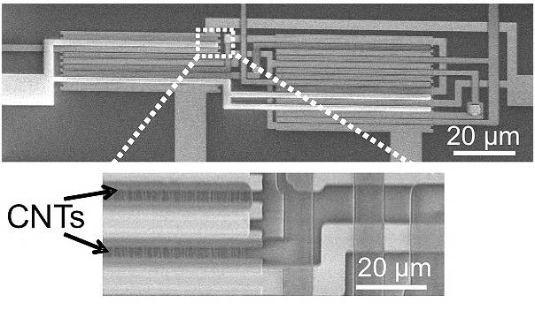 |
| An electron microscope image showing carbon nanotube transistors (CNTs) arranged in an integrated logic circuit. |
Abstract:
New techniques for preventing flaws, building multilayer chips result in prototypes that demonstrate feasibility of "nanotube" logic circuits.
New Stanford techniques make carbon-based integrated circuits more practical
Stanford, CA | Posted on December 28th, 2009Stanford engineers have built what they believe is a chip with the most advanced computing and storage elements made of carbon nanotubes to date by devising a way to root out the stubborn complication of nanotubes that cause short circuits.
Nanotubes, which resemble microscopic straws of rolled-up chicken wire, are widely viewed as the potential next generation of materials for enabling improved speed and energy efficiency of computer chips.
The researchers presented their results today at the International Electron Devices Meeting (IEDM) in Baltimore, along with another advance in using nanotubes to make multilayered, three-dimensional circuits.
"This body of work illustrates that carbon nanotube transistor technology has moved beyond the realm of scientific discovery and into engineering research," said H.-S. Philip Wong, a professor of electrical engineering at Stanford and a co-author of the paper. "We are now able to construct devices and build circuits on a wafer scale as opposed to previous 'one-of-a-kind' type demonstrations. Devices are in a circuit environment that is relevant to both today's and tomorrow's system needs."
The handful of nanotube transistors in the circuits the team fabricated can't compare to the hundreds of millions of transistors on a commercial microprocessor or memory chip, but their arrangement, the way they were made and their properties are much closer to commercial-grade than any nanotube devices made before, said Subhasish Mitra, an assistant professor of computer science and electrical engineering at Stanford.
The transistors are grouped in the same "cascading" sequences needed to produce computational logic and memory, and the process used to make them is compatible with the industrial VLSI (very large scale integration) manufacturing standard.
"We are very pleased with the rapid progress being made by Professors Wong and Mitra and their research teams in developing these technologies to help overcome barriers to further integration of complex carbon-based electronic circuits, which will lead to more useful products for future generations," said Betsy Weitzman, executive vice president and director of the Semiconductor Research Corporation's Focus Center Research Program, which helped fund the research, along with the National Science Foundation.
The chips employ three advanced techniques invented at Stanford to overcome endemic problems associated with nanotubes. One, invented in 2007, allows transistors to work regardless of whether the component nanotubes lie perfectly straight. Another, invented in 2008, enables VLSI-scale fabrication of nanotube transistors on a chip. The one announced today at the IEDM, is a process for reliably removing nanotubes that always conduct electrical current even when they are not supposed to. Such troublesome "metallic" nanotubes can short-circuit transistors if they aren't removed. The difficulty researchers have faced is finding ways to remove all the troublesome nanotubes, without damaging any other part of a circuit, including the nanotubes that behave properly.
The new technique, which the researchers call VLSI-compatible Metallic Nanotube Removal (VMR), builds upon an idea first proposed by Paul Collins and colleagues at IBM in 2001. That idea was to break up the nanotubes by exposing them to high current. The Stanford team has now made the idea practical on a VLSI scale by creating a grid of electrodes that zap away the unwanted nanotubes. That same electrode grid can then be etched to produce any circuit design, including ones that make use of the Stanford-developed techniques mentioned above.
The lead author on the VMR paper presented at IEDM is electrical engineering Stanford graduate student Nishant Patil. Other authors include electrical engineering graduate students Albert Lin, Jie Zhang and Hai Wei, and undergraduate student Kyle Anderson.
3-D nanotube circuits
Five members of the team (Wei, Patil, Lin, Wong and Mitra) immediately followed up the VMR paper at IEDM with another presentation describing the first multilayer carbon nanotube three-dimensionally integrated circuit.
Like multilevel parking garages, three-dimensional circuits allow for packing of more units - in this case, transistors - into a confined area. On chips, the third dimension can also reduce the lengths of some interconnecting wires, reducing energy required for data transmission. While engineers have recently begun making progress in building three-dimensional circuits by stacking and connecting layers made with conventional materials, the Stanford work shows it can be done with nanotubes in a way that is integrated from the start as a 3-D design, yielding a higher density of connections among layers.
Indicating that progress may be possible with nanotubes, the Stanford researchers were able to fashion a prototype three-layer chip with dozens of nanotube transistors that were connected in functioning logic gates by nanotube and metal wiring. What made the feat possible, Mitra said, was the use of a relatively low-temperature process that the researchers developed last year in which nanotubes are transferred from a quartz wafer onto a silicon chip.
A remaining challenge is to increase the number of nanotubes that can be properly patterned on a given area of a chip, to allow for making the millions of transistors that modern designs require. That's not a hurdle that researchers expect to leave unleapt.
Both projects were supported by the Focus Center Research Program and the National Science Foundation's Directorate for Computer and Information Science and Engineering (CISE).
"NSF and in particular CISE, is very interested in exploring exciting new avenues of obtaining continued hardware performance improvements beyond the limits of Moore's Law," said Sampath Kannan, a CISE division director at the National Science Foundation.
"The team led by Professors Mitra and Wong, supported by several grants from CISE, is pioneering research along one of these avenues. Their new results on VLSI-scale technique to deal with metallic carbon nanotubes for circuit design and their experimental demonstration of imperfection-immune VLSI-compatible CNT circuits take us closer to making integrated circuits using carbon nanotubes a practical reality."
David Orenstein is the communications and public relations manager at the School of Engineering.
####
About Stanford
Located between San Francisco and San Jose in the heart of Silicon Valley, Stanford University is recognized as one of the world's leading research and teaching institutions.
Leland and Jane Stanford founded the University to "promote the public welfare by exercising an influence on behalf of humanity and civilization." Stanford opened its doors in 1891, and more than a century later, it remains dedicated to finding solutions to the great challenges of the day and to preparing our students for leadership in today's complex world.
For more information, please click here
Contacts:
David Orenstein
Stanford Engineering
(650) 736-2245
Copyright © Stanford
If you have a comment, please Contact us.Issuers of news releases, not 7th Wave, Inc. or Nanotechnology Now, are solely responsible for the accuracy of the content.
Bookmark:


| Related News Press |
News and information
![]() Quantum computer improves AI predictions April 17th, 2026
Quantum computer improves AI predictions April 17th, 2026
![]() Flexible sensor gains sensitivity under pressure April 17th, 2026
Flexible sensor gains sensitivity under pressure April 17th, 2026
![]() A reusable chip for particulate matter sensing April 17th, 2026
A reusable chip for particulate matter sensing April 17th, 2026
![]() Detecting vibrational quantum beating in the predissociation dynamics of SF6 using time-resolved photoelectron spectroscopy April 17th, 2026
Detecting vibrational quantum beating in the predissociation dynamics of SF6 using time-resolved photoelectron spectroscopy April 17th, 2026
Possible Futures
![]() A fundamentally new therapeutic approach to cystic fibrosis: Nanobody repairs cellular defect April 17th, 2026
A fundamentally new therapeutic approach to cystic fibrosis: Nanobody repairs cellular defect April 17th, 2026
![]() UC Irvine physicists discover method to reverse �quantum scrambling� : The work addresses the problem of information loss in quantum computing system April 17th, 2026
UC Irvine physicists discover method to reverse �quantum scrambling� : The work addresses the problem of information loss in quantum computing system April 17th, 2026
Chip Technology
![]() A reusable chip for particulate matter sensing April 17th, 2026
A reusable chip for particulate matter sensing April 17th, 2026
![]() Metasurfaces smooth light to boost magnetic sensing precision January 30th, 2026
Metasurfaces smooth light to boost magnetic sensing precision January 30th, 2026
Nanotubes/Buckyballs/Fullerenes/Nanorods/Nanostrings/Nanosheets
![]() Tiny nanosheets, big leap: A new sensor detects ethanol at ultra-low levels January 30th, 2026
Tiny nanosheets, big leap: A new sensor detects ethanol at ultra-low levels January 30th, 2026
![]() Enhancing power factor of p- and n-type single-walled carbon nanotubes April 25th, 2025
Enhancing power factor of p- and n-type single-walled carbon nanotubes April 25th, 2025
![]() Chainmail-like material could be the future of armor: First 2D mechanically interlocked polymer exhibits exceptional flexibility and strength January 17th, 2025
Chainmail-like material could be the future of armor: First 2D mechanically interlocked polymer exhibits exceptional flexibility and strength January 17th, 2025
![]() Innovative biomimetic superhydrophobic coating combines repair and buffering properties for superior anti-erosion December 13th, 2024
Innovative biomimetic superhydrophobic coating combines repair and buffering properties for superior anti-erosion December 13th, 2024
Nanoelectronics
![]() Lab to industry: InSe wafer-scale breakthrough for future electronics August 8th, 2025
Lab to industry: InSe wafer-scale breakthrough for future electronics August 8th, 2025
![]() Interdisciplinary: Rice team tackles the future of semiconductors Multiferroics could be the key to ultralow-energy computing October 6th, 2023
Interdisciplinary: Rice team tackles the future of semiconductors Multiferroics could be the key to ultralow-energy computing October 6th, 2023
![]() Key element for a scalable quantum computer: Physicists from Forschungszentrum J�lich and RWTH Aachen University demonstrate electron transport on a quantum chip September 23rd, 2022
Key element for a scalable quantum computer: Physicists from Forschungszentrum J�lich and RWTH Aachen University demonstrate electron transport on a quantum chip September 23rd, 2022
![]() Reduced power consumption in semiconductor devices September 23rd, 2022
Reduced power consumption in semiconductor devices September 23rd, 2022
Announcements
![]() A fundamentally new therapeutic approach to cystic fibrosis: Nanobody repairs cellular defect April 17th, 2026
A fundamentally new therapeutic approach to cystic fibrosis: Nanobody repairs cellular defect April 17th, 2026
![]() UC Irvine physicists discover method to reverse �quantum scrambling� : The work addresses the problem of information loss in quantum computing system April 17th, 2026
UC Irvine physicists discover method to reverse �quantum scrambling� : The work addresses the problem of information loss in quantum computing system April 17th, 2026
Grants/Sponsored Research/Awards/Scholarships/Gifts/Contests/Honors/Records
![]() Quantum computer improves AI predictions April 17th, 2026
Quantum computer improves AI predictions April 17th, 2026
![]() Detecting vibrational quantum beating in the predissociation dynamics of SF6 using time-resolved photoelectron spectroscopy April 17th, 2026
Detecting vibrational quantum beating in the predissociation dynamics of SF6 using time-resolved photoelectron spectroscopy April 17th, 2026
![]() Metasurfaces smooth light to boost magnetic sensing precision January 30th, 2026
Metasurfaces smooth light to boost magnetic sensing precision January 30th, 2026
|
|
||
|
|
||
| The latest news from around the world, FREE | ||
|
|
||
|
|
||
| Premium Products | ||
|
|
||
|
Only the news you want to read!
Learn More |
||
|
|
||
|
Full-service, expert consulting
Learn More |
||
|
|
||