Home > Press > Thermochemical Nanolithograpy Now Allows Multiple Chemicals on Chip
 |
Abstract:
Scientists at Georgia Tech have developed a nanolithographic technique that can produce high-resolution patterns of at least three different chemicals on a single chip at writing speeds of up to one millimeter per second.
Thermochemical Nanolithograpy Now Allows Multiple Chemicals on Chip
Atlanta, GA | Posted on December 16th, 2009The chemical nanopatterns can be tailor-designed with any desired shape and have been shown to be sufficiently stable so that they can be stored for weeks and then used elsewhere. The technique, known as Thermochemical Nanolithography is detailed in the December 2009 edition of the journal Advanced Functional Materials. The research has applications in a number of scientific fields from electronics to medicine.
"The strength of this method is really the possibility to produce low-cost, high-resolution and high-density chemical patterns on a sample that can be delivered in any lab around the world, where even non experts in nanotechnology can dip the sample in the desired solution and, for example, make nano-arrays of proteins, DNA or nanoparticles," said Elisa Riedo, associate professor in the School of Physics at the Georgia Institute of Technology.
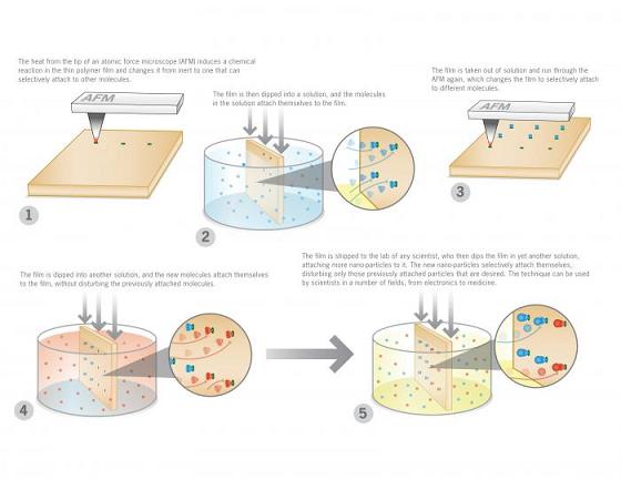
Conceptually, the technique is surprisingly simple. Using an atomic force microscope (AFM), researchers heat a silicon tip and run it over a thin polymer film. The heat from the tip induces a local chemical reaction at the surface of the film. This reaction changes the film's chemical reactivity and transforms it from an inert surface to a reactive one that can selectively attach other molecules. The team first developed the technique in 2007. Now they've added some important new twists that should make thermochemical nanolithography (TCNL) an extremely useful tool for scientists working at the nanoscale.
"We've created a way to make independent patterns of multiple chemicals on a chip that can be drawn in whatever shape you want," said Jennifer Curtis, assistant professor in the School of Physics.
Being able to create high-resolution features of different chemicals in arbitrary shapes is important because some nanolithography techniques are limited to just one chemistry, lower resolutions and/or fixed shapes. In addition, TCNL's speed capability of one millimeter per second makes it orders of magnitude faster than the widely used dip-pen nanolithography, which routinely clocks at a speed of 0.0001 millimeters per second per pen.
The research is enabled by heated AFM probe tips that can create a hot spot as small as a few nanometers in diameter. Such tips are designed and fabricated by collaborator Professor William King at the University of Illinois, Urbana-Champaign. "The heated tip allows one to direct nano-scale chemical reactions," said King.
The new technique produces multiple chemical patterns on the same chip by using the AFM to heat a polymer film and change its reactivity. The chip is then dipped into a solution, which allows chemicals (for example, proteins or other chemical linkers) in the solution to bind to the chip on the parts where it has been heated. The AFM then heats the film in another spot. The chip is dipped into another solution and again another chemical can bind to the chip.
In the paper, the scientists show they can pattern amine, thiol, aldehyde and biotin using this technique. But in principle TCNL could be used for almost any chemical. Their work also shows that the chemical patterns can be used to organize functional materials at the surface, such as proteins and DNA.
"The power of this technique is that in principle it can work with almost any chemical or chemically reactive nano-object. It allows scientists to very rapidly draw many things that can then be converted to any number of different things, which themselves can bind selectively to yet any number of other things. So, it doesn't matter if you're interested in biology, electronics, medicine or chemistry, TCNL can create the reactive pattern to bind what you choose," said Seth Marder, professor in Tech's School of Chemistry and Biochemistry and director of the Center for Organic Photonics and Electronics.
In addition, TCNL allows the chemical writing to be done in one location with the nano-object patterning in another, so that scientists who aren't experts in writing chemical patterns on the nanoscale can still attach their objects to it. It's the technique's stability that makes this possible.
"Once you draw the pattern, it's very stable and non-reactive. We've shown that you can have it for more than a month, take it out and dip it and it still will bind," said Riedo.
"I would like to think that several years from now people will have access to a TCNL tool that enables them to do this patterning at a place like Georgia Tech, that's much less expensive than the kind of nanolithography tools we currently use in our clean room," said Marder.
The research was supported by the National Science Foundation, the U.S. Department of Energy, the Georgia Institute of Technology, GT Innovative Award, and ONR Nanoelectronics.
####
About Georgia Tech
The Georgia Institute of Technology is one of the nation's premier research universities. Ranked seventh among U.S. News & World Report's top public universities, Georgia Tech's more than 19,000 students are enrolled in its Colleges of Architecture, Computing, Engineering, Liberal Arts, Management and Sciences. Tech is among the nation's top producers of women and African-American engineers. The Institute offers research opportunities to both undergraduate and graduate students and is home to more than 100 interdisciplinary units plus the Georgia Tech Research Institute.
For more information, please click here
Contacts:
David Terraso
Communications and Marketing
404-385-2966
Copyright © Georgia Tech
If you have a comment, please Contact us.Issuers of news releases, not 7th Wave, Inc. or Nanotechnology Now, are solely responsible for the accuracy of the content.
Bookmark:


| Related News Press |
News and information
![]() Quantum computer improves AI predictions April 17th, 2026
Quantum computer improves AI predictions April 17th, 2026
![]() Flexible sensor gains sensitivity under pressure April 17th, 2026
Flexible sensor gains sensitivity under pressure April 17th, 2026
![]() A reusable chip for particulate matter sensing April 17th, 2026
A reusable chip for particulate matter sensing April 17th, 2026
![]() Detecting vibrational quantum beating in the predissociation dynamics of SF6 using time-resolved photoelectron spectroscopy April 17th, 2026
Detecting vibrational quantum beating in the predissociation dynamics of SF6 using time-resolved photoelectron spectroscopy April 17th, 2026
Chemistry
![]() Projecting light to dispense liquids: A new route to ultra-precise microdroplets January 30th, 2026
Projecting light to dispense liquids: A new route to ultra-precise microdroplets January 30th, 2026
![]() From sensors to smart systems: the rise of AI-driven photonic noses January 30th, 2026
From sensors to smart systems: the rise of AI-driven photonic noses January 30th, 2026
![]() "Nanoreactor" cage uses visible light for catalytic and ultra-selective cross-cycloadditions October 3rd, 2025
"Nanoreactor" cage uses visible light for catalytic and ultra-selective cross-cycloadditions October 3rd, 2025
![]() Cambridge chemists discover simple way to build bigger molecules � one carbon at a time June 6th, 2025
Cambridge chemists discover simple way to build bigger molecules � one carbon at a time June 6th, 2025
Govt.-Legislation/Regulation/Funding/Policy
![]() Quantum computer improves AI predictions April 17th, 2026
Quantum computer improves AI predictions April 17th, 2026
![]() Metasurfaces smooth light to boost magnetic sensing precision January 30th, 2026
Metasurfaces smooth light to boost magnetic sensing precision January 30th, 2026
![]() New imaging approach transforms study of bacterial biofilms August 8th, 2025
New imaging approach transforms study of bacterial biofilms August 8th, 2025
Possible Futures
![]() A fundamentally new therapeutic approach to cystic fibrosis: Nanobody repairs cellular defect April 17th, 2026
A fundamentally new therapeutic approach to cystic fibrosis: Nanobody repairs cellular defect April 17th, 2026
![]() UC Irvine physicists discover method to reverse �quantum scrambling� : The work addresses the problem of information loss in quantum computing system April 17th, 2026
UC Irvine physicists discover method to reverse �quantum scrambling� : The work addresses the problem of information loss in quantum computing system April 17th, 2026
Nanomedicine
![]() A fundamentally new therapeutic approach to cystic fibrosis: Nanobody repairs cellular defect April 17th, 2026
A fundamentally new therapeutic approach to cystic fibrosis: Nanobody repairs cellular defect April 17th, 2026
![]() New molecular technology targets tumors and simultaneously silences two �undruggable� cancer genes August 8th, 2025
New molecular technology targets tumors and simultaneously silences two �undruggable� cancer genes August 8th, 2025
![]() New imaging approach transforms study of bacterial biofilms August 8th, 2025
New imaging approach transforms study of bacterial biofilms August 8th, 2025
![]() Electrifying results shed light on graphene foam as a potential material for lab grown cartilage June 6th, 2025
Electrifying results shed light on graphene foam as a potential material for lab grown cartilage June 6th, 2025
Nanoelectronics
![]() Lab to industry: InSe wafer-scale breakthrough for future electronics August 8th, 2025
Lab to industry: InSe wafer-scale breakthrough for future electronics August 8th, 2025
![]() Interdisciplinary: Rice team tackles the future of semiconductors Multiferroics could be the key to ultralow-energy computing October 6th, 2023
Interdisciplinary: Rice team tackles the future of semiconductors Multiferroics could be the key to ultralow-energy computing October 6th, 2023
![]() Key element for a scalable quantum computer: Physicists from Forschungszentrum J�lich and RWTH Aachen University demonstrate electron transport on a quantum chip September 23rd, 2022
Key element for a scalable quantum computer: Physicists from Forschungszentrum J�lich and RWTH Aachen University demonstrate electron transport on a quantum chip September 23rd, 2022
![]() Reduced power consumption in semiconductor devices September 23rd, 2022
Reduced power consumption in semiconductor devices September 23rd, 2022
Announcements
![]() A fundamentally new therapeutic approach to cystic fibrosis: Nanobody repairs cellular defect April 17th, 2026
A fundamentally new therapeutic approach to cystic fibrosis: Nanobody repairs cellular defect April 17th, 2026
![]() UC Irvine physicists discover method to reverse �quantum scrambling� : The work addresses the problem of information loss in quantum computing system April 17th, 2026
UC Irvine physicists discover method to reverse �quantum scrambling� : The work addresses the problem of information loss in quantum computing system April 17th, 2026
Nanobiotechnology
![]() A fundamentally new therapeutic approach to cystic fibrosis: Nanobody repairs cellular defect April 17th, 2026
A fundamentally new therapeutic approach to cystic fibrosis: Nanobody repairs cellular defect April 17th, 2026
![]() New molecular technology targets tumors and simultaneously silences two �undruggable� cancer genes August 8th, 2025
New molecular technology targets tumors and simultaneously silences two �undruggable� cancer genes August 8th, 2025
![]() New imaging approach transforms study of bacterial biofilms August 8th, 2025
New imaging approach transforms study of bacterial biofilms August 8th, 2025
![]() Electrifying results shed light on graphene foam as a potential material for lab grown cartilage June 6th, 2025
Electrifying results shed light on graphene foam as a potential material for lab grown cartilage June 6th, 2025
|
|
||
|
|
||
| The latest news from around the world, FREE | ||
|
|
||
|
|
||
| Premium Products | ||
|
|
||
|
Only the news you want to read!
Learn More |
||
|
|
||
|
Full-service, expert consulting
Learn More |
||
|
|
||