Home > Press > Imec presents new GaN-on-Si architecture for enhancement mode power switching devices
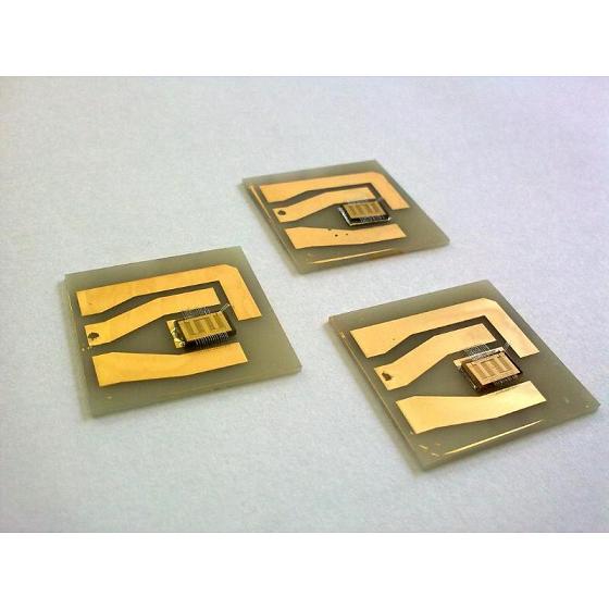 |
| IMEC SiN/AlGaN/GaN field effect transistor |
Abstract:
At this week's International Electron Devices Meeting, the nanoelectronics research center imec presents an innovative, simple and robust GaN-on-Si double heterostructure FET (field effect transistor) architecture for GaN-on-Si power switching devices. The architecture meets the normally off requirements of power switching circuits and is characterized by low leakage and high breakdown voltage, both essential parameters to reduce the power loss of high-power switching applications.
Imec presents new GaN-on-Si architecture for enhancement mode power switching devices
IEEE IEDM 2009, Baltimore, MD | Posted on December 8th, 2009High-voltage power devices are traditionally based on Si-MOSFET structures. However, for a number of applications, Si power devices have reached the intrinsic material limits. GaN-compounds are nowadays the best candidates to replace Si power devices, thanks to their high band gap (excellent transport properties) and their high electrical breakdown field. However, the cost of GaN power devices is high. GaN-epilayers grown on large diameter Si wafers, potentially up to 200mm, offer a lower cost technology compared to other substrates.
Imec obtained a high-breakdown voltage of almost 1000V combined with low on-resistance by growing an SiN/AlGaN/GaN/AlGaN double heterostructure FET structure on a Si substrate. By combining its double heterostructure FET architecture with in-situ SiN grown in the same epitaxial sequence as the III-nitride layers, imec succeeded in obtaining e-mode device operation. This is typically required in applications for safety reasons. The fabrication is based on an optimized process for the selective removal of in-situ SiN. The resulting SiN/AlGaN/GaN/AlGaN double heterostructure FET is characterized by a high breakdown voltage of 980V, an excellent uniformity and a low dynamic specific on-resistance of 3.5 mW.cm2 that is well within the present state-of-the-art. These results hold the promise of a huge market opportunity for GaN-on-Si power devices.
Within imec's industrial affiliation program (IIAP) on GaN-on-Si technology, imec and its partners focus on the development of GaN technology for both power conversion and solid state lighting applications. An important goal of the program is to lower GaN technology cost by using large-diameter GaN-on-Si and hence by leveraging on the scale of economics. Imec invites both integrated device manufacturers and compound semiconductor industry to join the program. Partners can build on imec's extensive expertise in GaN and benefit from sharing of cost, risk and talent.
####
About IMEC
Imec performs world-leading research in nano-electronics. imec leverages its scientific knowledge with the innovative power of its global partnerships in ICT, healthcare and energy. imec delivers industry-relevant technology solutions. In a unique high-tech environment, its international top talent is committed to providing the building blocks for a better life in a sustainable society.
Imec is headquartered in Leuven, Belgium, and has offices in Belgium, the Netherlands, Taiwan, US, China and Japan. Its staff of more than 1,650 people includes over 550 industrial residents and guest researchers. In 2008, imec's revenue (P&L) was 270 million euro.
Further information on imec can be found at www.imec.be.
NOTE: Imec is a registered trademark for the activities of imec International (a legal entity set up under Belgian law as a "stichting van openbaar nut�), imec Belgium (imec vzw supported by the Flemish Government), imec the Netherlands (Stichting imec Nederland, part of Holst Centre which is supported by the Dutch Government) and imec Taiwan (imec Taiwan Co.).
For more information, please click here
Contacts:
Hanne Degans, IMEC Press Officer, T: +32 16 28 17 69,
Barbara Kalkis, Maestro Marketing & PR, T: +1 408 996 9975,
Copyright © IMEC
If you have a comment, please Contact us.Issuers of news releases, not 7th Wave, Inc. or Nanotechnology Now, are solely responsible for the accuracy of the content.
Bookmark:


| Related News Press |
News and information
![]() Quantum computer improves AI predictions April 17th, 2026
Quantum computer improves AI predictions April 17th, 2026
![]() Flexible sensor gains sensitivity under pressure April 17th, 2026
Flexible sensor gains sensitivity under pressure April 17th, 2026
![]() A reusable chip for particulate matter sensing April 17th, 2026
A reusable chip for particulate matter sensing April 17th, 2026
![]() Detecting vibrational quantum beating in the predissociation dynamics of SF6 using time-resolved photoelectron spectroscopy April 17th, 2026
Detecting vibrational quantum beating in the predissociation dynamics of SF6 using time-resolved photoelectron spectroscopy April 17th, 2026
Chip Technology
![]() A reusable chip for particulate matter sensing April 17th, 2026
A reusable chip for particulate matter sensing April 17th, 2026
![]() Metasurfaces smooth light to boost magnetic sensing precision January 30th, 2026
Metasurfaces smooth light to boost magnetic sensing precision January 30th, 2026
Nanoelectronics
![]() Lab to industry: InSe wafer-scale breakthrough for future electronics August 8th, 2025
Lab to industry: InSe wafer-scale breakthrough for future electronics August 8th, 2025
![]() Interdisciplinary: Rice team tackles the future of semiconductors Multiferroics could be the key to ultralow-energy computing October 6th, 2023
Interdisciplinary: Rice team tackles the future of semiconductors Multiferroics could be the key to ultralow-energy computing October 6th, 2023
![]() Key element for a scalable quantum computer: Physicists from Forschungszentrum J�lich and RWTH Aachen University demonstrate electron transport on a quantum chip September 23rd, 2022
Key element for a scalable quantum computer: Physicists from Forschungszentrum J�lich and RWTH Aachen University demonstrate electron transport on a quantum chip September 23rd, 2022
![]() Reduced power consumption in semiconductor devices September 23rd, 2022
Reduced power consumption in semiconductor devices September 23rd, 2022
Announcements
![]() A fundamentally new therapeutic approach to cystic fibrosis: Nanobody repairs cellular defect April 17th, 2026
A fundamentally new therapeutic approach to cystic fibrosis: Nanobody repairs cellular defect April 17th, 2026
![]() UC Irvine physicists discover method to reverse �quantum scrambling� : The work addresses the problem of information loss in quantum computing system April 17th, 2026
UC Irvine physicists discover method to reverse �quantum scrambling� : The work addresses the problem of information loss in quantum computing system April 17th, 2026
Events/Classes
![]() Institute for Nanoscience hosts annual proposal planning meeting May 16th, 2025
Institute for Nanoscience hosts annual proposal planning meeting May 16th, 2025
![]() A New Blue: Mysterious origin of the ribbontail ray�s electric blue spots revealed July 5th, 2024
A New Blue: Mysterious origin of the ribbontail ray�s electric blue spots revealed July 5th, 2024
![]() Researchers demonstrate co-propagation of quantum and classical signals: Study shows that quantum encryption can be implemented in existing fiber networks January 20th, 2023
Researchers demonstrate co-propagation of quantum and classical signals: Study shows that quantum encryption can be implemented in existing fiber networks January 20th, 2023
|
|
||
|
|
||
| The latest news from around the world, FREE | ||
|
|
||
|
|
||
| Premium Products | ||
|
|
||
|
Only the news you want to read!
Learn More |
||
|
|
||
|
Full-service, expert consulting
Learn More |
||
|
|
||