Home > Press > Single-atom transistor discovered
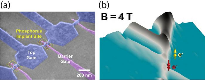 |
| (a) Colored scanning electron microscope image of the measured device. Aluminum top gate is used to induce a two-dimensional electron layer at the silicon-silicon oxide interface below the metallization. The barrier gate is partially below the top gate and depletes the electron layer in the vicinity of the phosphorus donors (the red spheres added to the original image). The barrier gate can also be used to control the conductivity of the device. All the barrier gates in the figure form their own individual transistors. (b) Measured differential conductance through the device at 4 Tesla magnetic field. The red and the yellow spheres illustrate the spin-down and -up states of a donor electron which induce the lines of high conductivity clearly visible in the figure. Courtesy and Copyright Helsinki University of Technology |
Abstract:
Researchers from Helsinki University of Technology (Finland), University of New South Wales (Australia), and University of Melbourne (Australia) have succeeded in building a working transistor, whose active region composes only of a single phosphorus atom in silicon. The results have just been published in Nano Letters.
Single-atom transistor discovered
Finland & Australia | Posted on December 5th, 2009The working principles of the device are based on sequential tunneling of single electrons between the phosphorus atom and the source and drain leads of the transistor. The tunneling can be suppressed or allowed by controlling the voltage on a nearby metal electrode with a width of a few tens of nanometers.
The rapid development of computers, which created the present information society, has been mainly based on the reduction of the size of transistors. We have known for a long time that this development has to slow down critically during the future decades when the even tighter inexpensive packing of transistors would require them to shrink down to the atomic length scales. In the recently developed transistor, all the electric current passes through the same single atom. This allows us to study the effects arising in the extreme limit of the transistor size.
"About half a year ago, I and one of the leaders of this research, Prof. Andrew Dzurak, were asked when we expect a single-atom transistor to be fabricated. We looked at each other, smiled, and said that we have already done that", tells Dr. Mikko M�tt�nen. "In fact, our purpose was not to build the tiniest transistor for a classical computer, but a quantum bit which would be the heart of a quantum computer that is being developed worldwide", he continues.
Problems arising when the size of a transistor is shrunk towards the ultimate limit are due to the emergence of so-called quantum mechanical effects. On one hand, these phenomena are expected to challenge the usual transistor operation. On the other hand, they allow classically irrational behavior which can, in principle, be harnessed for conceptually more efficient computing, quantum computing. The driving force behind the measurements reported now is the idea to utilize the spin degree of freedom of an electron of the phosphorus donor as a quantum bit, a qubit. The researchers were able to observe in their experiments spin up and down states for a single phosphorus donor for the first time. This is a crucial step towards the control of these states, that is, the realization of a qubit.
Original research article has been published in Nano Letters on Dec. 1st, 2009: Transport Spectroscopy of Single Phosphorus Donors in a Silicon Nanoscale Transistor, Kuan Yen Tan, Kok Wai Chan, Mikko M�tt�nen, Andrea Morello, Changyi Yang, Jessica van Donkelaar, Andrew Alves, Juha Matti Pirkkalainen, David N. Jamieson, Robert G. Clark, and Andrew S. Dzurak, Nano Lett., Article ASAP, DOI: 10.1021/nl901635j (2009). pubs.acs.org/doi/abs/10.1021/nl901635j
####
About Helsinki University of Technology
Helsinki University of Technology, TKK, is the oldest university of technology in Finland and a pioneer in the field of technology in the country: its fields of education and research cover all areas of technology that are of importance to the Finnish economy, including architecture.TKK is committed to the provision of high-quality education. We aim to equip our students with a firm foundation of knowledge needed in various fields of technology to enable their continuous professional development and ensure that they meet the requirements of an increasingly international operating environment. Our commitment has not gone unnoticed: we have been designated as a University of Excellence both in adult education and in research. Although we focus on technology and natural sciences, we should not forget art; our department of Architecture successfully keeps up the traditions of Finnish architecture.
For more information, please click here
Contacts:
Dr. Mikko M�tt�nen, Helsinki University of Technology, Department of Applied Physics, tel. +358 9 470 22342 or +358 50 594 0950
Prof. Andrew Dzurak, University of New South Wales, Centre for Quantum Computer Technology, a.dzurak [at] unsw.edu.au, tel. +61293856311
Copyright © Helsinki University of Technology
If you have a comment, please Contact us.Issuers of news releases, not 7th Wave, Inc. or Nanotechnology Now, are solely responsible for the accuracy of the content.
Bookmark:


| Related News Press |
News and information
![]() Quantum computer improves AI predictions April 17th, 2026
Quantum computer improves AI predictions April 17th, 2026
![]() Flexible sensor gains sensitivity under pressure April 17th, 2026
Flexible sensor gains sensitivity under pressure April 17th, 2026
![]() A reusable chip for particulate matter sensing April 17th, 2026
A reusable chip for particulate matter sensing April 17th, 2026
![]() Detecting vibrational quantum beating in the predissociation dynamics of SF6 using time-resolved photoelectron spectroscopy April 17th, 2026
Detecting vibrational quantum beating in the predissociation dynamics of SF6 using time-resolved photoelectron spectroscopy April 17th, 2026
Chip Technology
![]() A reusable chip for particulate matter sensing April 17th, 2026
A reusable chip for particulate matter sensing April 17th, 2026
![]() Metasurfaces smooth light to boost magnetic sensing precision January 30th, 2026
Metasurfaces smooth light to boost magnetic sensing precision January 30th, 2026
Quantum Computing
![]() Quantum computer improves AI predictions April 17th, 2026
Quantum computer improves AI predictions April 17th, 2026
![]() UC Irvine physicists discover method to reverse �quantum scrambling� : The work addresses the problem of information loss in quantum computing system April 17th, 2026
UC Irvine physicists discover method to reverse �quantum scrambling� : The work addresses the problem of information loss in quantum computing system April 17th, 2026
![]() Researchers develop molecular qubits that communicate at telecom frequencies October 3rd, 2025
Researchers develop molecular qubits that communicate at telecom frequencies October 3rd, 2025
Nanoelectronics
![]() Lab to industry: InSe wafer-scale breakthrough for future electronics August 8th, 2025
Lab to industry: InSe wafer-scale breakthrough for future electronics August 8th, 2025
![]() Interdisciplinary: Rice team tackles the future of semiconductors Multiferroics could be the key to ultralow-energy computing October 6th, 2023
Interdisciplinary: Rice team tackles the future of semiconductors Multiferroics could be the key to ultralow-energy computing October 6th, 2023
![]() Key element for a scalable quantum computer: Physicists from Forschungszentrum J�lich and RWTH Aachen University demonstrate electron transport on a quantum chip September 23rd, 2022
Key element for a scalable quantum computer: Physicists from Forschungszentrum J�lich and RWTH Aachen University demonstrate electron transport on a quantum chip September 23rd, 2022
![]() Reduced power consumption in semiconductor devices September 23rd, 2022
Reduced power consumption in semiconductor devices September 23rd, 2022
Announcements
![]() A fundamentally new therapeutic approach to cystic fibrosis: Nanobody repairs cellular defect April 17th, 2026
A fundamentally new therapeutic approach to cystic fibrosis: Nanobody repairs cellular defect April 17th, 2026
![]() UC Irvine physicists discover method to reverse �quantum scrambling� : The work addresses the problem of information loss in quantum computing system April 17th, 2026
UC Irvine physicists discover method to reverse �quantum scrambling� : The work addresses the problem of information loss in quantum computing system April 17th, 2026
Quantum nanoscience
![]() Beyond silicon: Electronics at the scale of a single molecule January 30th, 2026
Beyond silicon: Electronics at the scale of a single molecule January 30th, 2026
![]() MXene nanomaterials enter a new dimension Multilayer nanomaterial: MXene flakes created at Drexel University show new promise as 1D scrolls January 30th, 2026
MXene nanomaterials enter a new dimension Multilayer nanomaterial: MXene flakes created at Drexel University show new promise as 1D scrolls January 30th, 2026
![]() ICFO researchers overcome long-standing bottleneck in single photon detection with twisted 2D materials August 8th, 2025
ICFO researchers overcome long-standing bottleneck in single photon detection with twisted 2D materials August 8th, 2025
|
|
||
|
|
||
| The latest news from around the world, FREE | ||
|
|
||
|
|
||
| Premium Products | ||
|
|
||
|
Only the news you want to read!
Learn More |
||
|
|
||
|
Full-service, expert consulting
Learn More |
||
|
|
||