Home > Press > Nanowires key to future transistors, electronics
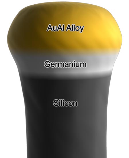 |
| Researchers are closer to using tiny devices called semiconducting nanowires to create a new generation of ultrasmall transistors and more powerful computer chips. The researchers have grown the nanowires with sharply defined layers of silicon and germanium, offering better transistor performance. As depicted in this illustration, tiny particles of a gold-aluminum alloy were alternately heated and cooled inside a vacuum chamber, and then silicon and germanium gases were alternately introduced. As the gold-aluminum bead absorbed the gases, it became "supersaturated" with silicon and germanium, causing them to precipitate and form wires. (Purdue University, Birck Nanotechnology Center/Seyet LLC) |
Abstract:
A new generation of ultrasmall transistors and more powerful computer chips using tiny structures called semiconducting nanowires are closer to reality after a key discovery by researchers at IBM, Purdue University and the University of California at Los Angeles.
Nanowires key to future transistors, electronics
West Lafayette, IN | Posted on November 27th, 2009The researchers have learned how to create nanowires with layers of different materials that are sharply defined at the atomic level, which is a critical requirement for making efficient transistors out of the structures.
"Having sharply defined layers of materials enables you to improve and control the flow of electrons and to switch this flow on and off," said Eric Stach, an associate professor of materials engineering at Purdue.
Electronic devices are often made of "heterostructures," meaning they contain sharply defined layers of different semiconducting materials, such as silicon and germanium. Until now, however, researchers have been unable to produce nanowires with sharply defined silicon and germanium layers. Instead, this transition from one layer to the next has been too gradual for the devices to perform optimally as transistors.
The new findings point to a method for creating nanowire transistors.
The findings are detailed in a research paper appearing Friday (Nov. 27) in the journal Science. The paper was written by Purdue postdoctoral researcher Cheng-Yen Wen, Stach, IBM materials scientists Frances Ross, Jerry Tersoff and Mark Reuter at the Thomas J. Watson Research Center in Yorktown Heights, N.Y, and Suneel Kodambaka, an assistant professor at UCLA's Department of Materials Science and Engineering.
Whereas conventional transistors are made on flat, horizontal pieces of silicon, the silicon nanowires are "grown" vertically. Because of this vertical structure, they have a smaller footprint, which could make it possible to fit more transistors on an integrated circuit, or chip, Stach said.
"But first we need to learn how to manufacture nanowires to exacting standards before industry can start using them to produce transistors," he said.
Nanowires might enable engineers to solve a problem threatening to derail the electronics industry. New technologies will be needed for industry to maintain Moore's law, an unofficial rule stating that the number of transistors on a computer chip doubles about every 18 months, resulting in rapid progress in computers and telecommunications. Doubling the number of devices that can fit on a computer chip translates into a similar increase in performance. However, it is becoming increasingly difficult to continue shrinking electronic devices made of conventional silicon-based semiconductors.
"In something like five to, at most, 10 years, silicon transistor dimensions will have been scaled to their limit," Stach said.
Transistors made of nanowires represent one potential way to continue the tradition of Moore's law.
The researchers used an instrument called a transmission electron microscope to observe the nanowire formation. Tiny particles of a gold-aluminum alloy were first heated and melted inside a vacuum chamber, and then silicon gas was introduced into the chamber. As the melted gold-aluminum bead absorbed the silicon, it became "supersaturated" with silicon, causing the silicon to precipitate and form wires. Each growing wire was topped with a liquid bead of gold-aluminum so that the structure resembled a mushroom.
Then, the researchers reduced the temperature inside the chamber enough to cause the gold-aluminum cap to solidify, allowing germanium to be deposited onto the silicon precisely and making it possible to create a heterostructure of silicon and germanium.
The cycle could be repeated, switching the gases from germanium to silicon as desired to make specific types of heterostructures, Stach said.
Having a heterostructure makes it possible to create a germanium "gate" in each transistor, which enables devices to switch on and off.
The work is based at IBM's Thomas J. Watson Research Center and Purdue's Birck Nanotechnology Center in the university's Discovery Park and is funded by the National Science Foundation through the NSF's Electronic and Photonic Materials Program in the Division of Materials Research.
ABSTRACT
Formation of Compositionally Abrupt Axial Heterojunctions in Si/Ge Nanowires
C.-Y. Wen1, M. C. Reuter2, J. Bruley2, J. Tersoff2, S. Kodambaka3, E. A. Stach1 and F. M. Ross2
1Purdue University, School of Materials Engineering and Birck Nanotechnology Center, West Lafayette, IN; 2IBM T. J. Watson Research Center, Yorktown Heights, NY; Yorktown Heights, NY; 3University of California Los Angeles, Department of Materials Science and Engineering, Los Angeles, CA.
We have formed compositionally abrupt interfaces in Si/Ge and Si/SiGe heterostructure nanowires by using solid AlAu alloy catalyst particles rather than the conventional liquid semiconductor/metal eutectic droplets. We demonstrate single interfaces that are defect-free and close to atomically abrupt, as well as quantum dots, i.e. Ge layers tens of atomic planes thick embedded within Si wires. We show, through real time imaging of growth kinetics, that a low solubility of Si and Ge in the solid particle accounts for the interfacial abruptness, and we discuss the use of solid catalysts to form functional group IV nanowire-based structures for an extended range of electronic applications.
####
About Purdue University
In addition to its academic programs offered at Purdue's campuses, the College of Technology offers learning programs at several other locations in the state of Indiana.
For more information, please click here
Contacts:
Writer
Emil Venere
(765) 494-4709
Source
Eric Stach
(765) 494-1466
Purdue News Service
(765) 494-2096
Copyright © Purdue University
If you have a comment, please Contact us.Issuers of news releases, not 7th Wave, Inc. or Nanotechnology Now, are solely responsible for the accuracy of the content.
Bookmark:


| Related News Press |
News and information
![]() Quantum computer improves AI predictions April 17th, 2026
Quantum computer improves AI predictions April 17th, 2026
![]() Flexible sensor gains sensitivity under pressure April 17th, 2026
Flexible sensor gains sensitivity under pressure April 17th, 2026
![]() A reusable chip for particulate matter sensing April 17th, 2026
A reusable chip for particulate matter sensing April 17th, 2026
![]() Detecting vibrational quantum beating in the predissociation dynamics of SF6 using time-resolved photoelectron spectroscopy April 17th, 2026
Detecting vibrational quantum beating in the predissociation dynamics of SF6 using time-resolved photoelectron spectroscopy April 17th, 2026
Govt.-Legislation/Regulation/Funding/Policy
![]() Quantum computer improves AI predictions April 17th, 2026
Quantum computer improves AI predictions April 17th, 2026
![]() Metasurfaces smooth light to boost magnetic sensing precision January 30th, 2026
Metasurfaces smooth light to boost magnetic sensing precision January 30th, 2026
![]() New imaging approach transforms study of bacterial biofilms August 8th, 2025
New imaging approach transforms study of bacterial biofilms August 8th, 2025
Chip Technology
![]() A reusable chip for particulate matter sensing April 17th, 2026
A reusable chip for particulate matter sensing April 17th, 2026
![]() Metasurfaces smooth light to boost magnetic sensing precision January 30th, 2026
Metasurfaces smooth light to boost magnetic sensing precision January 30th, 2026
Nanoelectronics
![]() Lab to industry: InSe wafer-scale breakthrough for future electronics August 8th, 2025
Lab to industry: InSe wafer-scale breakthrough for future electronics August 8th, 2025
![]() Interdisciplinary: Rice team tackles the future of semiconductors Multiferroics could be the key to ultralow-energy computing October 6th, 2023
Interdisciplinary: Rice team tackles the future of semiconductors Multiferroics could be the key to ultralow-energy computing October 6th, 2023
![]() Key element for a scalable quantum computer: Physicists from Forschungszentrum J�lich and RWTH Aachen University demonstrate electron transport on a quantum chip September 23rd, 2022
Key element for a scalable quantum computer: Physicists from Forschungszentrum J�lich and RWTH Aachen University demonstrate electron transport on a quantum chip September 23rd, 2022
![]() Reduced power consumption in semiconductor devices September 23rd, 2022
Reduced power consumption in semiconductor devices September 23rd, 2022
Discoveries
![]() Quantum computer improves AI predictions April 17th, 2026
Quantum computer improves AI predictions April 17th, 2026
![]() Flexible sensor gains sensitivity under pressure April 17th, 2026
Flexible sensor gains sensitivity under pressure April 17th, 2026
![]() A reusable chip for particulate matter sensing April 17th, 2026
A reusable chip for particulate matter sensing April 17th, 2026
![]() Detecting vibrational quantum beating in the predissociation dynamics of SF6 using time-resolved photoelectron spectroscopy April 17th, 2026
Detecting vibrational quantum beating in the predissociation dynamics of SF6 using time-resolved photoelectron spectroscopy April 17th, 2026
Announcements
![]() A fundamentally new therapeutic approach to cystic fibrosis: Nanobody repairs cellular defect April 17th, 2026
A fundamentally new therapeutic approach to cystic fibrosis: Nanobody repairs cellular defect April 17th, 2026
![]() UC Irvine physicists discover method to reverse �quantum scrambling� : The work addresses the problem of information loss in quantum computing system April 17th, 2026
UC Irvine physicists discover method to reverse �quantum scrambling� : The work addresses the problem of information loss in quantum computing system April 17th, 2026
Tools
![]() Metasurfaces smooth light to boost magnetic sensing precision January 30th, 2026
Metasurfaces smooth light to boost magnetic sensing precision January 30th, 2026
![]() From sensors to smart systems: the rise of AI-driven photonic noses January 30th, 2026
From sensors to smart systems: the rise of AI-driven photonic noses January 30th, 2026
![]() Japan launches fully domestically produced quantum computer: Expo visitors to experience quantum computing firsthand August 8th, 2025
Japan launches fully domestically produced quantum computer: Expo visitors to experience quantum computing firsthand August 8th, 2025
|
|
||
|
|
||
| The latest news from around the world, FREE | ||
|
|
||
|
|
||
| Premium Products | ||
|
|
||
|
Only the news you want to read!
Learn More |
||
|
|
||
|
Full-service, expert consulting
Learn More |
||
|
|
||