Home > Press > Pinning Down Superconductivity to a Single Layer
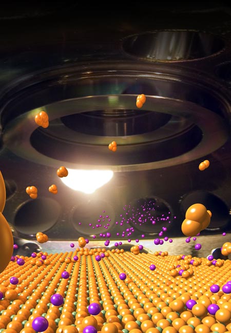 |
| This graphic shows the inside of the molecular beam epitaxy chamber where thin films are built layer by layer, showing an artists rendition of the film synthesis process. |
Abstract:
Findings may lead to precision engineering of superconducting thin films for electronic devices
Pinning Down Superconductivity to a Single Layer
Upton, NY | Posted on October 30th, 2009Using precision techniques for making superconducting thin films layer-by-layer, physicists at the U.S. Department of Energy's (DOE) Brookhaven National Laboratory have identified a single layer responsible for one such material's ability to become superconducting, i.e., carry electrical current with no energy loss. The technique, described in the October 30, 2009, issue of Science, could be used to engineer ultrathin films with "tunable" superconductivity for higher-efficiency electronic devices.
"We wanted to answer a fundamental question about such films," said Brookhaven physicist and the group leader Ivan Bozovic. "Namely: How thin can the film be and still retain high-temperature superconductivity?"
The thinner the material (and the higher its transition temperature to a superconductor), the greater its potential for applications where the superconductivity can be controlled by an external electric field. "This type of control is difficult to achieve with thicker films, because an electric field does not penetrate into metals more than a nanometer or so," Bozovic explained.
To explore the limits of thinness, Bozovic's group synthesized a series of films based on the high-temperature superconducting cuprates (copper-oxides) � materials that carry current with no energy loss when cooled below a certain transition temperature (Tc). Since zinc is known to suppress the superconductivity in these materials, the scientists systematically substituted a small amount of zinc into each of the copper-oxide layers. Any layer where the zinc's presence had a suppressing effect would be clearly identified as essential to superconductivity in the film.
"Our measurements showed that the zinc doping had essentially no effect, except when placed in a single, well-defined layer. When the zinc was in that layer, the superconductivity was dramatically suppressed," Bozovic said.
The material studied by Bozovic's team was unusual in that it consists of layers of two materials, one metallic and one insulating, that are not superconductors on their own, but rather exhibit superconductivity at the interface between them.
The layer identified as essential to the superconductivity by the zinc-substitution experiment represents the second copper-oxide layer away from the interface. The scientists found that the presence of zinc had no effect on the transition temperature at which superconductivity sets in, about 32 kelvin (-241 Celsius), except when placed in that particular layer. In the latter case, the scientists observed a dramatic drop in the transition temperature to 18 kelvin (-255 Celsius). The reduction in transition temperature provides a clear indication that that particular layer is the "hot" one responsible for the relatively high temperature at which superconductivity normally sets in for this material.
"We now have a clean experimental proof that high-temperature superconductivity can exist, undiminished, in a single copper-oxide layer," Bozovic said. "This piece of information gives important input to our theoretical understanding of this phenomenon."
Bozovic explained that, in the material he studied, the electrons required for superconductivity actually come from the metallic material below the interface. They leak into the insulating material above the interface and achieve the critical level in that second copper-oxide layer.
But in principle, he says, there are other ways to achieve the same concentration of electrons in that single layer, for example, by doping achieved by applying electric fields. That would result in high-temperature superconductivity in a single copper-oxide layer measuring just 0.66 nanometers.
From a practical viewpoint, this discovery opens a path toward the fabrication of electronic devices with modulated, or tunable, superconducting properties which can be controlled by electric or magnetic fields.
"Electronic devices already consume a large fraction of our electricity usage � and this is growing fast." Bozovic continued. "Clearly, we will need less-power hungry electronics in the future." Superconductors, which operate without energy loss � particularly those that operate at warmer, more-practical temperatures � may be one way to go.
Bozovic's layer-by-layer synthesis method and ability to strategically alter individual layers' composition might also be used to explore and possibly control other electronic phenomena and properties that emerge at the interfaces between layered materials.
This research was funded by the DOE Office of Science.
####
About Brookhaven National Laboratories
One of ten national laboratories overseen and primarily funded by the Office of Science of the U.S. Department of Energy (DOE), Brookhaven National Laboratory conducts research in the physical, biomedical, and environmental sciences, as well as in energy technologies and national security. Brookhaven Lab also builds and operates major scientific facilities available to university, industry and government researchers. Brookhaven is operated and managed for DOE's Office of Science by Brookhaven Science Associates, a limited-liability company founded by Stony Brook University, the largest academic user of Laboratory facilities, and Battelle, a nonprofit, applied science and technology organization.
For more information, please click here
Contacts:
Karen McNulty Walsh
(631) 344-8350
Mona S. Rowe
(631) 344-5056
Copyright © Brookhaven National Laboratories
If you have a comment, please Contact us.Issuers of news releases, not 7th Wave, Inc. or Nanotechnology Now, are solely responsible for the accuracy of the content.
Bookmark:


| Related News Press |
News and information
![]() Quantum computer improves AI predictions April 17th, 2026
Quantum computer improves AI predictions April 17th, 2026
![]() Flexible sensor gains sensitivity under pressure April 17th, 2026
Flexible sensor gains sensitivity under pressure April 17th, 2026
![]() A reusable chip for particulate matter sensing April 17th, 2026
A reusable chip for particulate matter sensing April 17th, 2026
![]() Detecting vibrational quantum beating in the predissociation dynamics of SF6 using time-resolved photoelectron spectroscopy April 17th, 2026
Detecting vibrational quantum beating in the predissociation dynamics of SF6 using time-resolved photoelectron spectroscopy April 17th, 2026
Physics
![]() UC Irvine physicists discover method to reverse �quantum scrambling� : The work addresses the problem of information loss in quantum computing system April 17th, 2026
UC Irvine physicists discover method to reverse �quantum scrambling� : The work addresses the problem of information loss in quantum computing system April 17th, 2026
![]() Quantum computers simulate fundamental physics: shedding light on the building blocks of nature June 6th, 2025
Quantum computers simulate fundamental physics: shedding light on the building blocks of nature June 6th, 2025
![]() A 1960s idea inspires NBI researchers to study hitherto inaccessible quantum states June 6th, 2025
A 1960s idea inspires NBI researchers to study hitherto inaccessible quantum states June 6th, 2025
Thin films
![]() Tiny nanosheets, big leap: A new sensor detects ethanol at ultra-low levels January 30th, 2026
Tiny nanosheets, big leap: A new sensor detects ethanol at ultra-low levels January 30th, 2026
Govt.-Legislation/Regulation/Funding/Policy
![]() Quantum computer improves AI predictions April 17th, 2026
Quantum computer improves AI predictions April 17th, 2026
![]() Metasurfaces smooth light to boost magnetic sensing precision January 30th, 2026
Metasurfaces smooth light to boost magnetic sensing precision January 30th, 2026
![]() New imaging approach transforms study of bacterial biofilms August 8th, 2025
New imaging approach transforms study of bacterial biofilms August 8th, 2025
Possible Futures
![]() A fundamentally new therapeutic approach to cystic fibrosis: Nanobody repairs cellular defect April 17th, 2026
A fundamentally new therapeutic approach to cystic fibrosis: Nanobody repairs cellular defect April 17th, 2026
![]() UC Irvine physicists discover method to reverse �quantum scrambling� : The work addresses the problem of information loss in quantum computing system April 17th, 2026
UC Irvine physicists discover method to reverse �quantum scrambling� : The work addresses the problem of information loss in quantum computing system April 17th, 2026
Chip Technology
![]() A reusable chip for particulate matter sensing April 17th, 2026
A reusable chip for particulate matter sensing April 17th, 2026
![]() Metasurfaces smooth light to boost magnetic sensing precision January 30th, 2026
Metasurfaces smooth light to boost magnetic sensing precision January 30th, 2026
Nanoelectronics
![]() Lab to industry: InSe wafer-scale breakthrough for future electronics August 8th, 2025
Lab to industry: InSe wafer-scale breakthrough for future electronics August 8th, 2025
![]() Interdisciplinary: Rice team tackles the future of semiconductors Multiferroics could be the key to ultralow-energy computing October 6th, 2023
Interdisciplinary: Rice team tackles the future of semiconductors Multiferroics could be the key to ultralow-energy computing October 6th, 2023
![]() Key element for a scalable quantum computer: Physicists from Forschungszentrum J�lich and RWTH Aachen University demonstrate electron transport on a quantum chip September 23rd, 2022
Key element for a scalable quantum computer: Physicists from Forschungszentrum J�lich and RWTH Aachen University demonstrate electron transport on a quantum chip September 23rd, 2022
![]() Reduced power consumption in semiconductor devices September 23rd, 2022
Reduced power consumption in semiconductor devices September 23rd, 2022
Discoveries
![]() Quantum computer improves AI predictions April 17th, 2026
Quantum computer improves AI predictions April 17th, 2026
![]() Flexible sensor gains sensitivity under pressure April 17th, 2026
Flexible sensor gains sensitivity under pressure April 17th, 2026
![]() A reusable chip for particulate matter sensing April 17th, 2026
A reusable chip for particulate matter sensing April 17th, 2026
![]() Detecting vibrational quantum beating in the predissociation dynamics of SF6 using time-resolved photoelectron spectroscopy April 17th, 2026
Detecting vibrational quantum beating in the predissociation dynamics of SF6 using time-resolved photoelectron spectroscopy April 17th, 2026
Announcements
![]() A fundamentally new therapeutic approach to cystic fibrosis: Nanobody repairs cellular defect April 17th, 2026
A fundamentally new therapeutic approach to cystic fibrosis: Nanobody repairs cellular defect April 17th, 2026
![]() UC Irvine physicists discover method to reverse �quantum scrambling� : The work addresses the problem of information loss in quantum computing system April 17th, 2026
UC Irvine physicists discover method to reverse �quantum scrambling� : The work addresses the problem of information loss in quantum computing system April 17th, 2026
|
|
||
|
|
||
| The latest news from around the world, FREE | ||
|
|
||
|
|
||
| Premium Products | ||
|
|
||
|
Only the news you want to read!
Learn More |
||
|
|
||
|
Full-service, expert consulting
Learn More |
||
|
|
||