Home > Press > Rutgers Physicists Discover Novel Electronic Properties in Two-dimensional Carbon Structure
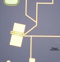 |
| Graphene sample with electrodes, fabricated using electron beam lithography |
Abstract:
Previously predicted but unobserved interactions between massless particles may lead to speedy, powerful electronic devices
Rutgers Physicists Discover Novel Electronic Properties in Two-dimensional Carbon Structure
New Brunswick, NJ | Posted on October 16th, 2009Rutgers researchers have discovered novel electronic properties in two-dimensional sheets of carbon atoms called graphene that could one day be the heart of speedy and powerful electronic devices.
The new findings, previously considered possible by physicists but only now being seen in the laboratory, show that electrons in graphene can interact strongly with each other. The behavior is similar to superconductivity observed in some metals and complex materials, marked by the flow of electric current with no resistance and other unusual but potentially useful properties. In graphene, this behavior results in a new liquid-like phase of matter consisting of fractionally charged quasi-particles, in which charge is transported with no dissipation.
In a paper issued online by the prestigious science journal Nature and slated for print publication in the coming weeks, physics professor Eva Andrei and her Rutgers colleagues note that the strong interaction between electrons, also called correlated behavior, had not been observed in graphene in spite of many attempts to coax it out. This led some scientists to question whether correlated behavior could even be possible in graphene, where the electrons are massless (ultra-relativistic) particles like photons and neutrinos. In most materials, electrons are particles that have mass.
"Our work demonstrated that earlier failures to observe correlated behavior were not due to the physical nature of graphene," said Eva Andrei, physics professor in the Rutgers School of Arts and Sciences. "Rather, it was because of interference from the material which supported graphene samples and the type of electrical probes used to study it."
This finding should encourage scientists to further pursue graphene and related materials for future electronic applications, including replacements for today's silicon-based semiconductor materials. Industry experts expect silicon technology to reach fundamental performance limits in a little more than a decade.
The Rutgers physicists further describe how they observed the collective behavior of the ultra-relativistic charge carriers in graphene through a phenomenon known as the fractional quantum Hall effect (FQHE). The FQHE is seen when charge carriers are confined to moving in a two-dimensional plane and are subject to a perpendicular magnetic field. When interactions between these charge carriers are sufficiently strong they form new quasi-particles with a fraction of an electron's elementary charge. The FHQE is the quintessential signature of strongly correlated behavior among charge-carrying particles in two dimensions.
The FHQE is known to exist in semiconductor-based, two-dimensional electron systems, where the electrons are massive particles that obey conventional dynamics versus the relativistic dynamics of massless particles. However, it was not obvious until now that ultra-relativistic electrons in graphene would be capable of exhibiting collective phenomena that give rise to the FHQE. The Rutgers physicists were surprised that the FHQE in graphene is even more robust than in standard semiconductors.
Scientists make graphene patches by rubbing graphite - the same material in ordinary pencil lead - onto a silicon wafer, which is a thin slice of silicon crystal used to make computer chips. Then they run electrical pathways to the graphene patches using ordinary integrated circuit fabrication techniques. While scientists were able to investigate many properties of the resulting graphene electronic device, they were not able to induce the sought-after fractional quantum Hall effect.
Andrei and her group proposed that impurities or irregularities in the thin layer of silicon dioxide underlying the graphene were preventing the scientists from achieving the exacting conditions they needed. Postdoctoral fellow Xu Du and undergraduate student Anthony Barker were able to show that etching out several layers of silicon dioxide below the graphene patches essentially leaves an intact graphene strip suspended in mid-air by the electrodes. This enabled the group to demonstrate that the carriers in suspended graphene essentially propagate ballistically without scattering from impurities. Another crucial step was to design and fabricate a probe geometry that did not interfere with measurements as Andrei suspected earlier ones were doing. These proved decisive steps to observing the correlated behavior in graphene.
In the past few months, other academic and corporate research groups have reported streamlined graphene production techniques, which will propel further research and potential applications.
Andrei's collaborators were Xu Du, now on faculty at Stony Brook University; Ivan Skachko, a post-doctoral fellow; Fabian Duerr, a master's student; and Adina Luican, a doctoral student. The research was supported by the Department of Energy, the National Science Foundation, the Institute for Complex Adaptive Matter and Alcatel-Lucent.
####
About Rutgers
Rutgers, The State University of New Jersey, is a leading national public research university and the state�s preeminent, comprehensive public institution of higher education. Rutgers is dedicated to teaching that meets the highest standards of excellence; to conducting research that breaks new ground; and to turning knowledge into solutions for local, national, and global communities.
As it was at our founding in 1766, the heart of our mission is preparing students to become productive members of society and good citizens of the world. Rutgers teaches across the full educational spectrum: preschool to precollege; undergraduate to graduate and postdoctoral; and continuing education for professional and personal advancement. Rutgers is New Jersey�s land-grant institution and one of the nation�s foremost research universities, and as such, we educate, make discoveries, serve as an engine of economic growth, and generate ideas for improving people�s lives.
For more information, please click here
Contacts:
Carl Blesch
732-932-7084 x616
Copyright © Rutgers
If you have a comment, please Contact us.Issuers of news releases, not 7th Wave, Inc. or Nanotechnology Now, are solely responsible for the accuracy of the content.
Bookmark:


| Related News Press |
News and information
![]() Quantum computer improves AI predictions April 17th, 2026
Quantum computer improves AI predictions April 17th, 2026
![]() Flexible sensor gains sensitivity under pressure April 17th, 2026
Flexible sensor gains sensitivity under pressure April 17th, 2026
![]() A reusable chip for particulate matter sensing April 17th, 2026
A reusable chip for particulate matter sensing April 17th, 2026
![]() Detecting vibrational quantum beating in the predissociation dynamics of SF6 using time-resolved photoelectron spectroscopy April 17th, 2026
Detecting vibrational quantum beating in the predissociation dynamics of SF6 using time-resolved photoelectron spectroscopy April 17th, 2026
Possible Futures
![]() A fundamentally new therapeutic approach to cystic fibrosis: Nanobody repairs cellular defect April 17th, 2026
A fundamentally new therapeutic approach to cystic fibrosis: Nanobody repairs cellular defect April 17th, 2026
![]() UC Irvine physicists discover method to reverse �quantum scrambling� : The work addresses the problem of information loss in quantum computing system April 17th, 2026
UC Irvine physicists discover method to reverse �quantum scrambling� : The work addresses the problem of information loss in quantum computing system April 17th, 2026
Chip Technology
![]() A reusable chip for particulate matter sensing April 17th, 2026
A reusable chip for particulate matter sensing April 17th, 2026
![]() Metasurfaces smooth light to boost magnetic sensing precision January 30th, 2026
Metasurfaces smooth light to boost magnetic sensing precision January 30th, 2026
Nanoelectronics
![]() Lab to industry: InSe wafer-scale breakthrough for future electronics August 8th, 2025
Lab to industry: InSe wafer-scale breakthrough for future electronics August 8th, 2025
![]() Interdisciplinary: Rice team tackles the future of semiconductors Multiferroics could be the key to ultralow-energy computing October 6th, 2023
Interdisciplinary: Rice team tackles the future of semiconductors Multiferroics could be the key to ultralow-energy computing October 6th, 2023
![]() Key element for a scalable quantum computer: Physicists from Forschungszentrum J�lich and RWTH Aachen University demonstrate electron transport on a quantum chip September 23rd, 2022
Key element for a scalable quantum computer: Physicists from Forschungszentrum J�lich and RWTH Aachen University demonstrate electron transport on a quantum chip September 23rd, 2022
![]() Reduced power consumption in semiconductor devices September 23rd, 2022
Reduced power consumption in semiconductor devices September 23rd, 2022
Announcements
![]() A fundamentally new therapeutic approach to cystic fibrosis: Nanobody repairs cellular defect April 17th, 2026
A fundamentally new therapeutic approach to cystic fibrosis: Nanobody repairs cellular defect April 17th, 2026
![]() UC Irvine physicists discover method to reverse �quantum scrambling� : The work addresses the problem of information loss in quantum computing system April 17th, 2026
UC Irvine physicists discover method to reverse �quantum scrambling� : The work addresses the problem of information loss in quantum computing system April 17th, 2026
Quantum nanoscience
![]() Beyond silicon: Electronics at the scale of a single molecule January 30th, 2026
Beyond silicon: Electronics at the scale of a single molecule January 30th, 2026
![]() MXene nanomaterials enter a new dimension Multilayer nanomaterial: MXene flakes created at Drexel University show new promise as 1D scrolls January 30th, 2026
MXene nanomaterials enter a new dimension Multilayer nanomaterial: MXene flakes created at Drexel University show new promise as 1D scrolls January 30th, 2026
![]() ICFO researchers overcome long-standing bottleneck in single photon detection with twisted 2D materials August 8th, 2025
ICFO researchers overcome long-standing bottleneck in single photon detection with twisted 2D materials August 8th, 2025
|
|
||
|
|
||
| The latest news from around the world, FREE | ||
|
|
||
|
|
||
| Premium Products | ||
|
|
||
|
Only the news you want to read!
Learn More |
||
|
|
||
|
Full-service, expert consulting
Learn More |
||
|
|
||