Home > Press > Simultaneous Nanoscale Imaging of Surface and Bulk Atoms
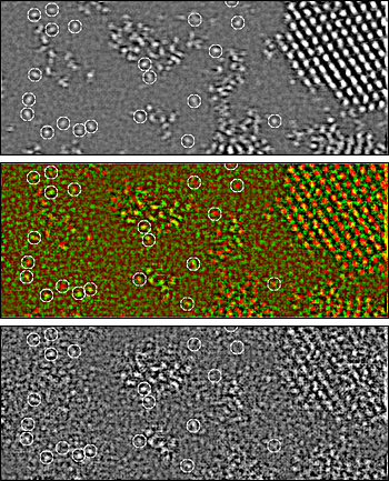 |
| Uranium single atoms (circled) and small crystallites on a carbon support imaged simultaneously using a scanning probe to produce forward scattering through the sample (top) and backward scattering emerging from the surface (bottom). Center panel shows superimposition of the two in red (bulk) and green (surface). Atoms not seen in the lower image are on the bottom surface of the support. |
Abstract:
New microscope could revolutionize imaging, improve catalysts for energy applications
Simultaneous Nanoscale Imaging of Surface and Bulk Atoms
Upton, NY | Posted on September 21st, 2009Scientists at the U.S. Department of Energy's (DOE) Brookhaven National Laboratory, in collaboration with researchers from Hitachi High Technologies Corp., have demonstrated a new scanning electron microscope capable of selectively imaging single atoms on the top surface of a specimen while a second, simultaneous imaging signal shows atoms throughout the sample's depth. This new tool, located at Brookhaven Lab's Center for Functional Nanomaterials (CFN), will greatly expand scientists' ability to understand and ultimately control chemical reactions, such as those of catalysts in energy-conversion devices.
A paper describing the work will be published online September 20, 2009, in Nature Materials, along with a commentary article highlighting the development.
"Our knowledge of the role of individual atoms in nanotechnology and energy-related research is strongly influenced by our ability to visualize them, not only in bulk but also on the surface, which is where the interactions of chemical reactions take place," said Brookhaven physicist Yimei Zhu, lead author on the paper. "This new microscope and the method we developed allow us, for the first time, to directly look at atoms on the top surface and in the bulk of a sample simultaneously to reveal their atomic arrangement and bonding states. This information will help us identify the active sites and functions of materials at nanoscale dimensions for a wide range of applications, such as converting waste heat or chemical energy to electricity."
Like all scanning electron microscopes, the new tool probes a sample with an electron beam focused to a tiny spot and detects so-called secondary electrons emitted by the sample to reveal its surface structure and topography. Though this technique has been a workhorse of surface imaging in industrial and academic laboratories for decades, its resolution has left much to be desired because of imperfect focusing due to lens aberrations.
Using a newly developed spherical aberration corrector, the new tool corrects these distortions to create a smaller probe with significantly increased brightness.
"The effect is similar to using a larger aperture lens on a camera," said biophysicst Joseph Wall, a longtime expert in electron microscopy at Brookhaven Lab and a co-author on the paper. "It allows you to gather information from a larger angle and focus on a smaller spot."
The new device also employs specialized electron optics to channel the emitted secondary electrons to the detector. The result is a fourfold improvement in resolution to below one tenth of a nanometer � and thus, the ability to image single atoms.
Additional detectors, located below the sample, detect electrons transmitted through the sample, revealing details about the entire structure at the exact instant the "shutter" snapped to record each pixel of the surface image. This simultaneous imaging allows the scientists to correlate information in the two images to understand precisely what is happening on the surface and throughout the sample at the same time.
"Having information about the surface structure and the bulk sample at the same time will allow researchers to better determine how the surface and bulk atoms work together, for example in a catalytic reaction," said Zhu. The improved resolution and combined imaging capabilities will also reveal features such as small variations in composition or the locations of impurities that could have large effects on function.
"An essential component of this study was selection of a test specimen, isolated uranium atoms on a thin carbon substrate, where the images could be interpreted quantitatively to rule out other possible interpretations," Wall commented.
Because of its extreme sensitivity, the new microscope must be kept isolated from a range of environmental effects such as variations in temperature, mechanical vibrations, and electromagnetic fields. Even the slightest waft of air could cause distortions in the images.
Fortunately the CFN was built with these needs in mind. Temperatures are regulated to within three-hundredths of a degree Fahrenheit over a 24-hour period; shock-absorber-like slabs isolate the room from the rumble of passing trucks and distant slamming doors; layers of heavy doors keep even subtle vibrations out; and air-cooling panels replace typical ceiling vents to eliminate airflow.
"The building is really a mechanical-engineering masterpiece," said Zhu. "This microscope wouldn't work at all without these sophisticated systems." Development of the microscope was funded by the Office of Basic Energy Sciences within the DOE Office of Science.
The Center for Functional Nanomaterials at Brookhaven National Laboratory is one of the five DOE Nanoscale Science Research Centers (NSRCs), premier national user facilities for interdisciplinary research at the nanoscale. Together the NSRCs comprise a suite of complementary facilities that provide researchers with state-of-the-art capabilities to fabricate, process, characterize and model nanoscale materials, and constitute the largest infrastructure investment of the National Nanotechnology Initiative. The NSRCs are located at DOE's Argonne, Brookhaven, Lawrence Berkeley, Oak Ridge and Sandia and Los Alamos national laboratories. For more information about the DOE NSRCs, please visit DOE's nanoscience website at www.science.doe.gov/news_information/news_room/2006/nano/index.htm
####
About Brookhaven National Laboratory
One of ten national laboratories overseen and primarily funded by the Office of Science of the U.S. Department of Energy (DOE), Brookhaven National Laboratory conducts research in the physical, biomedical, and environmental sciences, as well as in energy technologies and national security. Brookhaven Lab also builds and operates major scientific facilities available to university, industry and government researchers. Brookhaven is operated and managed for DOE's Office of Science by Brookhaven Science Associates, a limited-liability company founded by Stony Brook University, the largest academic user of Laboratory facilities, and Battelle, a nonprofit, applied science and technology organization.
For more information, please click here
Contacts:
Karen McNulty Walsh
(631) 344-8350
Mona S. Rowe
(631) 344-5056
Copyright © Brookhaven National Laboratory
If you have a comment, please Contact us.Issuers of news releases, not 7th Wave, Inc. or Nanotechnology Now, are solely responsible for the accuracy of the content.
Bookmark:


| Related News Press |
News and information
![]() Simulating magnetization in a Heisenberg quantum spin chain April 5th, 2024
Simulating magnetization in a Heisenberg quantum spin chain April 5th, 2024
![]() NRL charters Navy�s quantum inertial navigation path to reduce drift April 5th, 2024
NRL charters Navy�s quantum inertial navigation path to reduce drift April 5th, 2024
![]() Discovery points path to flash-like memory for storing qubits: Rice find could hasten development of nonvolatile quantum memory April 5th, 2024
Discovery points path to flash-like memory for storing qubits: Rice find could hasten development of nonvolatile quantum memory April 5th, 2024
Chemistry
![]() What heat can tell us about battery chemistry: using the Peltier effect to study lithium-ion cells March 8th, 2024
What heat can tell us about battery chemistry: using the Peltier effect to study lithium-ion cells March 8th, 2024
![]() Nanoscale CL thermometry with lanthanide-doped heavy-metal oxide in TEM March 8th, 2024
Nanoscale CL thermometry with lanthanide-doped heavy-metal oxide in TEM March 8th, 2024
Announcements
![]() NRL charters Navy�s quantum inertial navigation path to reduce drift April 5th, 2024
NRL charters Navy�s quantum inertial navigation path to reduce drift April 5th, 2024
![]() Discovery points path to flash-like memory for storing qubits: Rice find could hasten development of nonvolatile quantum memory April 5th, 2024
Discovery points path to flash-like memory for storing qubits: Rice find could hasten development of nonvolatile quantum memory April 5th, 2024
Tools
![]() Ferroelectrically modulate the Fermi level of graphene oxide to enhance SERS response November 3rd, 2023
Ferroelectrically modulate the Fermi level of graphene oxide to enhance SERS response November 3rd, 2023
![]() The USTC realizes In situ electron paramagnetic resonance spectroscopy using single nanodiamond sensors November 3rd, 2023
The USTC realizes In situ electron paramagnetic resonance spectroscopy using single nanodiamond sensors November 3rd, 2023
Energy
![]() Development of zinc oxide nanopagoda array photoelectrode: photoelectrochemical water-splitting hydrogen production January 12th, 2024
Development of zinc oxide nanopagoda array photoelectrode: photoelectrochemical water-splitting hydrogen production January 12th, 2024
![]() Shedding light on unique conduction mechanisms in a new type of perovskite oxide November 17th, 2023
Shedding light on unique conduction mechanisms in a new type of perovskite oxide November 17th, 2023
![]() Inverted perovskite solar cell breaks 25% efficiency record: Researchers improve cell efficiency using a combination of molecules to address different November 17th, 2023
Inverted perovskite solar cell breaks 25% efficiency record: Researchers improve cell efficiency using a combination of molecules to address different November 17th, 2023
![]() The efficient perovskite cells with a structured anti-reflective layer � another step towards commercialization on a wider scale October 6th, 2023
The efficient perovskite cells with a structured anti-reflective layer � another step towards commercialization on a wider scale October 6th, 2023
Alliances/Trade associations/Partnerships/Distributorships
![]() Chicago Quantum Exchange welcomes six new partners highlighting quantum technology solutions, from Chicago and beyond September 23rd, 2022
Chicago Quantum Exchange welcomes six new partners highlighting quantum technology solutions, from Chicago and beyond September 23rd, 2022
![]() University of Illinois Chicago joins Brookhaven Lab's Quantum Center June 10th, 2022
University of Illinois Chicago joins Brookhaven Lab's Quantum Center June 10th, 2022
|
|
||
|
|
||
| The latest news from around the world, FREE | ||
|
|
||
|
|
||
| Premium Products | ||
|
|
||
|
Only the news you want to read!
Learn More |
||
|
|
||
|
Full-service, expert consulting
Learn More |
||
|
|
||