Home > Press > Major step towards extremely sensitive chemical sensors
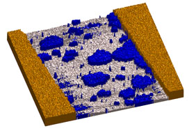 |
| Atomic force microscopy image of island growth in between two electrodes (left and right) of the SAMFET. The self-assembled monolayer islands, in the middle of the figure, conduct charges. In this case, no path is formed between the two electrodes and therefore current cannot flow. The height of the molecules is 3 nanometers; the length of the gap between the electrodes (i.e. the transistor channel length) is 5 microns. |
Abstract:
Together with colleagues from the Netherlands, Russia and Austria, researchers of TU/e gained a better understanding of the mechanism behind charge transport in SAMFETs. This opens the door to extremely sensitive chemical sensors, that could be produced in a cost-effective way. The findings were published online in Nature Nanotechnology.
Major step towards extremely sensitive chemical sensors
Eindhoven | Posted on August 14th, 2009The research was done at Philips Research Eindhoven and Eindhoven University of Technology.
SAMFETs
The SAMFET is a recent example of the development of �plastic micro-electronics'- i.e. electronics based on organic materials. Last year, Philips Research managed to build such a transistor by immersing a silicon substrate into solution containing liquid crystalline molecules that self-assemble onto this substrate, resulting in a semi-conductive layer of just a single molecule thick. The monolayer of the SAMFET consists of molecules that are standing upright. Conduction takes place by charges jumping from one molecule to the other.
However, in previous attempts to make a SAMFET, it was observed that as the length of the SAMFET increased, its level of conductivity counterintuitively decreased exponentially. In a joint project Philips Research, the Eindhoven University of Technology (TU/e), the University of Groningen, the Holst Centre, the Enikolopov Institute for Synthetical Polymer Materials in Moscow and the Technical University in Graz, Austria discovered that this decrease is determined by the monolayer coverage, which could be explained with a widely applicable two-dimensional percolation model.
The ultimate chemical sensor
One could compare this to crossing a river by jumping from rock to rock. The closer the rocks are to each other, the quicker one can jump or even walk to the other river bank. So if the monolayer displays more voids, the conductivity decreases dramatically. Up till now, this behavior was an uncharted area and inhibited the use of SAMFETs in applications such as sensors and plastic electronics. The SAMFET's extreme sensitivity could open doors to the development of the ultimate chemical sensor, the research team points out. "If we go back to that river again, another benefit of a SAMFET becomes clear", Martijn Kemerink, assistant professor at the TU/e indicates. "Imagine that there are just enough rocks to cross that river. When you remove just one rock, the effect is significant, for it is impossible to make it to the other side of the river. The SAMFET could be used to make sensors that give a large signal that is triggered by a small change", he continues.
Future steps
At present, SAMFETs are not widely used, for there are alternatives of which the production process is well-established. However, the production process of SAMFETs is extremely simple and material efficient. The transistor requires only a single layer of molecules that is applied by simple immersion into a chemical solution. The same solution can be used for many substrates, for the substrate only takes the necessary (small) amount of molecules. This makes future large-scale production of monolayer electronics efficient, simple and cost-effective.
Publication
The publication "Monolayer coverage and channel length set the mobility in self-assembled monolayer field-effect transistors", by Matthijssen et al. can be found at www.nature.com/nnano/journal/vaop/ncurrent/abs/nnano.2009.201.html.
The research was conducted at Philips Research Eindhoven and Eindhoven University of Technology. It was funded by STW, ONE-P, the Austrian Nanoinitiative en H.C. Starck GMBH.
####
About Eindhoven University of Technology
Eindhoven University of Technology (TU/e) intends to be a research driven, design oriented university of technology at an international level, with the primary objective of providing young people with an academic education within the �engineering science & technology� domain.
For more information, please click here
Contacts:
Den Dolech 2
P.O Box 513, 5600 MB Eindhoven
tel: 31(0)40-247 9111
fax: 31(0)40-245 6087
Copyright © Eindhoven University of Technology
If you have a comment, please Contact us.Issuers of news releases, not 7th Wave, Inc. or Nanotechnology Now, are solely responsible for the accuracy of the content.
Bookmark:


| Related News Press |
News and information
![]() Quantum computer improves AI predictions April 17th, 2026
Quantum computer improves AI predictions April 17th, 2026
![]() Flexible sensor gains sensitivity under pressure April 17th, 2026
Flexible sensor gains sensitivity under pressure April 17th, 2026
![]() A reusable chip for particulate matter sensing April 17th, 2026
A reusable chip for particulate matter sensing April 17th, 2026
![]() Detecting vibrational quantum beating in the predissociation dynamics of SF6 using time-resolved photoelectron spectroscopy April 17th, 2026
Detecting vibrational quantum beating in the predissociation dynamics of SF6 using time-resolved photoelectron spectroscopy April 17th, 2026
Possible Futures
![]() A fundamentally new therapeutic approach to cystic fibrosis: Nanobody repairs cellular defect April 17th, 2026
A fundamentally new therapeutic approach to cystic fibrosis: Nanobody repairs cellular defect April 17th, 2026
![]() UC Irvine physicists discover method to reverse �quantum scrambling� : The work addresses the problem of information loss in quantum computing system April 17th, 2026
UC Irvine physicists discover method to reverse �quantum scrambling� : The work addresses the problem of information loss in quantum computing system April 17th, 2026
Self Assembly
![]() Diamond glitter: A play of colors with artificial DNA crystals May 17th, 2024
Diamond glitter: A play of colors with artificial DNA crystals May 17th, 2024
![]() Liquid crystal templated chiral nanomaterials October 14th, 2022
Liquid crystal templated chiral nanomaterials October 14th, 2022
![]() Nanoclusters self-organize into centimeter-scale hierarchical assemblies April 22nd, 2022
Nanoclusters self-organize into centimeter-scale hierarchical assemblies April 22nd, 2022
![]() Atom by atom: building precise smaller nanoparticles with templates March 4th, 2022
Atom by atom: building precise smaller nanoparticles with templates March 4th, 2022
Sensors
![]() Flexible sensor gains sensitivity under pressure April 17th, 2026
Flexible sensor gains sensitivity under pressure April 17th, 2026
![]() Tiny nanosheets, big leap: A new sensor detects ethanol at ultra-low levels January 30th, 2026
Tiny nanosheets, big leap: A new sensor detects ethanol at ultra-low levels January 30th, 2026
![]() From sensors to smart systems: the rise of AI-driven photonic noses January 30th, 2026
From sensors to smart systems: the rise of AI-driven photonic noses January 30th, 2026
![]() Sensors innovations for smart lithium-based batteries: advancements, opportunities, and potential challenges August 8th, 2025
Sensors innovations for smart lithium-based batteries: advancements, opportunities, and potential challenges August 8th, 2025
Nanoelectronics
![]() Lab to industry: InSe wafer-scale breakthrough for future electronics August 8th, 2025
Lab to industry: InSe wafer-scale breakthrough for future electronics August 8th, 2025
![]() Interdisciplinary: Rice team tackles the future of semiconductors Multiferroics could be the key to ultralow-energy computing October 6th, 2023
Interdisciplinary: Rice team tackles the future of semiconductors Multiferroics could be the key to ultralow-energy computing October 6th, 2023
![]() Key element for a scalable quantum computer: Physicists from Forschungszentrum J�lich and RWTH Aachen University demonstrate electron transport on a quantum chip September 23rd, 2022
Key element for a scalable quantum computer: Physicists from Forschungszentrum J�lich and RWTH Aachen University demonstrate electron transport on a quantum chip September 23rd, 2022
![]() Reduced power consumption in semiconductor devices September 23rd, 2022
Reduced power consumption in semiconductor devices September 23rd, 2022
Announcements
![]() A fundamentally new therapeutic approach to cystic fibrosis: Nanobody repairs cellular defect April 17th, 2026
A fundamentally new therapeutic approach to cystic fibrosis: Nanobody repairs cellular defect April 17th, 2026
![]() UC Irvine physicists discover method to reverse �quantum scrambling� : The work addresses the problem of information loss in quantum computing system April 17th, 2026
UC Irvine physicists discover method to reverse �quantum scrambling� : The work addresses the problem of information loss in quantum computing system April 17th, 2026
Alliances/Trade associations/Partnerships/Distributorships
![]() Chicago Quantum Exchange welcomes six new partners highlighting quantum technology solutions, from Chicago and beyond September 23rd, 2022
Chicago Quantum Exchange welcomes six new partners highlighting quantum technology solutions, from Chicago and beyond September 23rd, 2022
![]() University of Illinois Chicago joins Brookhaven Lab's Quantum Center June 10th, 2022
University of Illinois Chicago joins Brookhaven Lab's Quantum Center June 10th, 2022
|
|
||
|
|
||
| The latest news from around the world, FREE | ||
|
|
||
|
|
||
| Premium Products | ||
|
|
||
|
Only the news you want to read!
Learn More |
||
|
|
||
|
Full-service, expert consulting
Learn More |
||
|
|
||