Home > Press > Novelx Wins Prestigious R&D 100 Award for Innovative Scanning Electron Microscope
 |
Abstract:
Novelx mySEM® miniaturizes and drives the cost out of field emission scanning electron microscopes to distribute nanoscale imaging capabilities more broadly.
Novelx Wins Prestigious R&D 100 Award for Innovative Scanning Electron Microscope
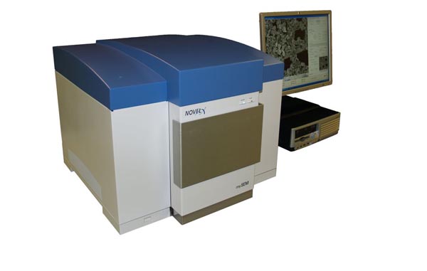
Lafayette, CA | Posted on July 21st, 2009Novelx, Inc. was just selected for a prestigious R&D 100 Award for one of the 100 most technologically significant new products in 2009. R&D Magazine recognized the Novelx mySEM® for miniaturizing and driving the cost out of the core technology inside a scanning electron microscope (SEM).
Powered by the patented Novelx Stacked Silicon Technology, the mySEM is a bench-top SEM for imaging and characterizing nanoscale objects and materials. In a compact design that installs easily into available lab space or closer to production lines, the mySEM delivers capabilities previously only available in high-end field emission SEMs, at a fraction of the cost. Optimized for low-voltage operation and without the need to coat non-conductive samples, the mySEM is an ideal choice for the imaging of energy sensitive nanomaterials, biomaterials, polymers, thin films and membranes.
Lawrence Muray, CEO and co-founder of Novelx, explains, "Novelx has designed and built a low cost, but high-performance compact field emission SEM. Our patented technology represents a disruptive innovation in how scanning electron microscopes are built and operated. By leveraging silicon processing technologies, Novelx has dramatically miniaturized the core technology inside a SEM. This miniaturization enabled the design of an all-electrostatic electron beam column that when coupled with a thermal field emission electron source is optimized for low-voltage imaging and sub-10nm resolution."
Several imaging techniques are available with the Novelx mySEM to enhance surface contrast and allow nanoscale features to be observed. A variable low-voltage system, the mySEM eliminates charging of non-conductive samples without the need to coat samples, which can mask many nanoscale features, or to operate at increased pressure, which can degrade resolution.
According to James Spallas, CTO and co-founder of the company, "The mySEM uses a quad-segmented microchannel plate (MCP) detector. This patent-pending detector can detect secondary and backscattered electrons together, backscattered electrons only, and can operate in a topographic mode that enhances surface topography. This topographic imaging technique is capable of sub-atomic vertical resolution of crystalline materials resulting in the ability to image individual dislocations, atomic steps and other defects on or near the surface."
Winners of the R&D 100 Awards are selected by an independent judging panel and the editors of R&D Magazine. According to Rita Peters, editorial director of R&D Magazine, "Winning an R&D 100 Award provides a mark of excellence known to industry, government, and academia as proof that the product is one of the most innovative ideas of the year."
The Novelx mySEM is commercially available and in use by several leading university research centers for the imaging of nanoscale objects and materials in a wide variety of fields that include Materials Science and the Life Sciences. Industrial applications include the characterization of nanomaterials at corporate product development labs, the failure analysis of nanoscale defects and the quality assurance of nanomaterial-based products closer to the production line.
####
About Novlex, Inc.
Novelx is a privately held corporation based in Lafayette, CA that builds the only compact field emission scanning electron microscope (SEM) available for imaging and characterizing nanoscale objects and materials. In a compact design that installs easily, the Novelx mySEM is optimized for low-voltage operation and delivers sub-10nm imaging capabilities previously only available in high-end field emission SEMs, at a fraction of the cost. The company’s patented Stacked Silicon technology is designed and built in California. More information can be found at www.novelx.com.
About R&D Magazine
Since its founding in 1959 as Industrial Research, R&D Magazine has served research scientists, engineers and technical staff at laboratories around the world, providing timely, informative news and useful technical articles that broaden readers’ knowledge of the research and development industry and improve the quality of their work. R&D Magazine is a publication of Advantage Business Media (www.advantagebusinessmedia.com).
mySEM is a registered trademark. The Novelx logo and Novelx Stacked Silicon Technology are trademarks of Novelx, Inc..
For more information, please click here
Contacts:
Jim Rynne
VP, Marketing and Business Development
Novelx, Inc.
+1 925.962.0889 x304
www.novelx.com
Copyright © Novlex, Inc.
If you have a comment, please Contact us.Issuers of news releases, not 7th Wave, Inc. or Nanotechnology Now, are solely responsible for the accuracy of the content.
Bookmark:


| Related News Press |
News and information
![]() Simulating magnetization in a Heisenberg quantum spin chain April 5th, 2024
Simulating magnetization in a Heisenberg quantum spin chain April 5th, 2024
![]() NRL charters Navy’s quantum inertial navigation path to reduce drift April 5th, 2024
NRL charters Navy’s quantum inertial navigation path to reduce drift April 5th, 2024
![]() Discovery points path to flash-like memory for storing qubits: Rice find could hasten development of nonvolatile quantum memory April 5th, 2024
Discovery points path to flash-like memory for storing qubits: Rice find could hasten development of nonvolatile quantum memory April 5th, 2024
Announcements
![]() NRL charters Navy’s quantum inertial navigation path to reduce drift April 5th, 2024
NRL charters Navy’s quantum inertial navigation path to reduce drift April 5th, 2024
![]() Discovery points path to flash-like memory for storing qubits: Rice find could hasten development of nonvolatile quantum memory April 5th, 2024
Discovery points path to flash-like memory for storing qubits: Rice find could hasten development of nonvolatile quantum memory April 5th, 2024
Tools
![]() Ferroelectrically modulate the Fermi level of graphene oxide to enhance SERS response November 3rd, 2023
Ferroelectrically modulate the Fermi level of graphene oxide to enhance SERS response November 3rd, 2023
![]() The USTC realizes In situ electron paramagnetic resonance spectroscopy using single nanodiamond sensors November 3rd, 2023
The USTC realizes In situ electron paramagnetic resonance spectroscopy using single nanodiamond sensors November 3rd, 2023
|
|
||
|
|
||
| The latest news from around the world, FREE | ||
|
|
||
|
|
||
| Premium Products | ||
|
|
||
|
Only the news you want to read!
Learn More |
||
|
|
||
|
Full-service, expert consulting
Learn More |
||
|
|
||