Home > Press > Statistical Technique Improves Nanotechnology Data
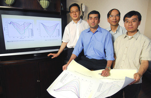 |
| Georgia Tech researchers illustrate how their new technique improves measurement of nanostructure properties. Shown (l-r) are Zhong Lin Wang, V. Roshan Joseph, C.F. Jeff Wu and Xinwei Deng. |
Abstract:
Improved Measurement Could Facilitate Industrial Applications
Statistical Technique Improves Nanotechnology Data
Atlanta, GA | Posted on July 1st, 2009A new statistical analysis technique that identifies and removes systematic bias, noise and equipment-based artifacts from experimental data could lead to more precise and reliable measurement of nanomaterials and nanostructures likely to have future industrial applications.
Known as sequential profile adjustment by regression (SPAR), the technique could also reduce the amount of experimental data required to make conclusions, and help distinguish true nanoscale phenomena from experimental error. Beyond nanomaterials and nanostructures, the technique could also improve reliability and precision in nanoelectronics measurements�and in studies of certain larger-scale systems.
Accurate understanding of these properties is critical to the development of future high-volume industrial applications for nanomaterials and nanostructures because manufacturers will require consistency in their products.
"Our statistical model will be useful when the nanomaterials industry scales up from laboratory production because industrial users cannot afford to make a detailed study of every production run," said C. F. Jeff Wu, a professor in the Stewart School of Industrial and Systems Engineering at the Georgia Institute of Technology. "The significant experimental errors can be filtered out automatically, which means this could be used in a manufacturing environment."
Sponsored by the National Science Foundation, the research was reported June 25, 2009 in the early edition of the journal Proceedings of the National Academy of Sciences. The paper is believed to be the first to describe the use of statistical techniques for quantitative analysis of data from nanomechanical measurements.
Nanotechnology researchers have long been troubled by the difficulty of measuring nanoscale properties and separating signals from noise and data artifacts. Data artifacts can be caused by such issues as the slippage of structures being studied, surface irregularities and inaccurate placement of the atomic force microscope tip onto samples.
In measuring the effects of extremely small forces acting on extremely small structures, signals of interest may be only two or three times stronger than experimental noise. That can make it difficult to draw conclusions, and potentially masks other interesting effects.
"In the past, we have really not known the statistical reliability of the data at this size scale," said Zhong Lin Wang, a Regents' professor in Georgia Tech's School of Materials Science and Engineering. "At the nanoscale, small errors are amplified. This new technique applies statistical theory to identify and analyze the data received from nanomechanics so we can be more confident of how reliable it is."
In developing the new technique, the researchers studied a data set measuring the deformation of zinc oxide nanobelts, research undertaken to determine the material's elastic modulus. Theoretically, applying force to a nanobelt with the tip of an atomic force microscope should produce consistent linear deformation, but the experimental data didn't always show that.
In some cases, less force appeared to create more deformation, and the deformation curve was not symmetrical. Wang's research team attempted to apply simple data-correction techniques, but was not satisfied with the results.
"The measurements they had done simply didn't match what was expected with the theoretical model," explained Wu, who holds a Coca-Cola chair in engineering statistics. "The curves should have been symmetric. To address this issue, we developed a new modeling technique that uses the data itself to filter out the mismatch step-by-step using the regression technique."
Ideally, researchers would search out and correct the experimental causes of these data errors, but because they occur at such small size scales, that would be difficult, noted V. Roshan Joseph, an associate professor in the Georgia Tech School of Industrial and Systems Engineering.
"Physics-based models are based on several assumptions that can go wrong in reality," he said. "We could try to identify all the sources of error and correct them, but that is very time-consuming. Statistical techniques can more easily correct the errors, so this process is more geared toward industrial use."
Beyond correcting the errors, the improved precision of the statistical technique could reduce the effort required to produce reliable experimental data on the properties of nanostructures. "With half of the experimental efforts, you can get about the same standard deviation as following the earlier method without the corrections," Wu said. "This translates into fewer time-consuming experiments to confirm the properties."
For the future, the research team�which includes Xinwei Deng and Wenjie Mai in addition to those already mentioned�plans to analyze the properties of nanowires, which are critical to the operation of a family of nanoscale electric generators being developed by Wang's research team. Correcting for data errors in these structures will require development of a separate model using the same SPAR techniques, Wu said.
Ultimately, SPAR may lead researchers to new fundamental explanations of the nanoscale world.
"One of the key issues today in nanotechnology is whether the existing physical theories can still be applied to explain the phenomena we are seeing," said Wang, who is also director of Georgia Tech's Center for Nanostructure Characterization and Fabrication. "We have tried to answer the question of whether we are truly observing new phenomena, or whether our errors are so large that we cannot see that the theory still works."
Wang plans to use the SPAR technique on future work, and to analyze past research for potential new findings. "What may have seemed like noise could actually be an important signal," he said. "This technique provides a truly new tool for data mining and analysis in nanotechnology."
####
About Georgia Institute of Technology
The Georgia Institute of Technology is one of the nation's premier research universities. Ranked seventh among U.S. News & World Report's top public universities, Georgia Tech's more than 19,000 students are enrolled in its Colleges of Architecture, Computing, Engineering, Liberal Arts, Management and Sciences. Tech is among the nation's top producers of women and African-American engineers. The Institute offers research opportunities to both undergraduate and graduate students and is home to more than 100 interdisciplinary units plus the Georgia Tech Research Institute.
For more information, please click here
Contacts:
Research News & Publications Office
Georgia Institute of Technology
75 Fifth Street, N.W., Suite 100
Atlanta, Georgia 30308 USA
Media Relations Assistance: John Toon 404-894-6986
or
Abby Vogel
404-385-3364
Copyright © Georgia Institute of Technology
If you have a comment, please Contact us.Issuers of news releases, not 7th Wave, Inc. or Nanotechnology Now, are solely responsible for the accuracy of the content.
Bookmark:


| Related News Press |
News and information
![]() Quantum computer improves AI predictions April 17th, 2026
Quantum computer improves AI predictions April 17th, 2026
![]() Flexible sensor gains sensitivity under pressure April 17th, 2026
Flexible sensor gains sensitivity under pressure April 17th, 2026
![]() A reusable chip for particulate matter sensing April 17th, 2026
A reusable chip for particulate matter sensing April 17th, 2026
![]() Detecting vibrational quantum beating in the predissociation dynamics of SF6 using time-resolved photoelectron spectroscopy April 17th, 2026
Detecting vibrational quantum beating in the predissociation dynamics of SF6 using time-resolved photoelectron spectroscopy April 17th, 2026
Possible Futures
![]() A fundamentally new therapeutic approach to cystic fibrosis: Nanobody repairs cellular defect April 17th, 2026
A fundamentally new therapeutic approach to cystic fibrosis: Nanobody repairs cellular defect April 17th, 2026
![]() UC Irvine physicists discover method to reverse �quantum scrambling� : The work addresses the problem of information loss in quantum computing system April 17th, 2026
UC Irvine physicists discover method to reverse �quantum scrambling� : The work addresses the problem of information loss in quantum computing system April 17th, 2026
Nanoelectronics
![]() Lab to industry: InSe wafer-scale breakthrough for future electronics August 8th, 2025
Lab to industry: InSe wafer-scale breakthrough for future electronics August 8th, 2025
![]() Interdisciplinary: Rice team tackles the future of semiconductors Multiferroics could be the key to ultralow-energy computing October 6th, 2023
Interdisciplinary: Rice team tackles the future of semiconductors Multiferroics could be the key to ultralow-energy computing October 6th, 2023
![]() Key element for a scalable quantum computer: Physicists from Forschungszentrum J�lich and RWTH Aachen University demonstrate electron transport on a quantum chip September 23rd, 2022
Key element for a scalable quantum computer: Physicists from Forschungszentrum J�lich and RWTH Aachen University demonstrate electron transport on a quantum chip September 23rd, 2022
![]() Reduced power consumption in semiconductor devices September 23rd, 2022
Reduced power consumption in semiconductor devices September 23rd, 2022
Materials/Metamaterials/Magnetoresistance
![]() First real-time observation of two-dimensional melting process: Researchers at Mainz University unveil new insights into magnetic vortex structures August 8th, 2025
First real-time observation of two-dimensional melting process: Researchers at Mainz University unveil new insights into magnetic vortex structures August 8th, 2025
![]() Researchers unveil a groundbreaking clay-based solution to capture carbon dioxide and combat climate change June 6th, 2025
Researchers unveil a groundbreaking clay-based solution to capture carbon dioxide and combat climate change June 6th, 2025
![]() A 1960s idea inspires NBI researchers to study hitherto inaccessible quantum states June 6th, 2025
A 1960s idea inspires NBI researchers to study hitherto inaccessible quantum states June 6th, 2025
![]() Institute for Nanoscience hosts annual proposal planning meeting May 16th, 2025
Institute for Nanoscience hosts annual proposal planning meeting May 16th, 2025
Announcements
![]() A fundamentally new therapeutic approach to cystic fibrosis: Nanobody repairs cellular defect April 17th, 2026
A fundamentally new therapeutic approach to cystic fibrosis: Nanobody repairs cellular defect April 17th, 2026
![]() UC Irvine physicists discover method to reverse �quantum scrambling� : The work addresses the problem of information loss in quantum computing system April 17th, 2026
UC Irvine physicists discover method to reverse �quantum scrambling� : The work addresses the problem of information loss in quantum computing system April 17th, 2026
Tools
![]() Metasurfaces smooth light to boost magnetic sensing precision January 30th, 2026
Metasurfaces smooth light to boost magnetic sensing precision January 30th, 2026
![]() From sensors to smart systems: the rise of AI-driven photonic noses January 30th, 2026
From sensors to smart systems: the rise of AI-driven photonic noses January 30th, 2026
![]() Japan launches fully domestically produced quantum computer: Expo visitors to experience quantum computing firsthand August 8th, 2025
Japan launches fully domestically produced quantum computer: Expo visitors to experience quantum computing firsthand August 8th, 2025
Industrial
![]() Tiny nanosheets, big leap: A new sensor detects ethanol at ultra-low levels January 30th, 2026
Tiny nanosheets, big leap: A new sensor detects ethanol at ultra-low levels January 30th, 2026
![]() Quantum interference in molecule-surface collisions February 28th, 2025
Quantum interference in molecule-surface collisions February 28th, 2025
![]() Boron nitride nanotube fibers get real: Rice lab creates first heat-tolerant, stable fibers from wet-spinning process June 24th, 2022
Boron nitride nanotube fibers get real: Rice lab creates first heat-tolerant, stable fibers from wet-spinning process June 24th, 2022
|
|
||
|
|
||
| The latest news from around the world, FREE | ||
|
|
||
|
|
||
| Premium Products | ||
|
|
||
|
Only the news you want to read!
Learn More |
||
|
|
||
|
Full-service, expert consulting
Learn More |
||
|
|
||