Home > Press > New focus for printed electronics
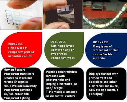 |
| Evolution of printed electronics structures
Source: IDTechEx with images from AIST, Waseda University and GE. |
Abstract:
In the last year, the burgeoning printed and thin film electronics industry has greatly enhanced its repertoire and changed its priorities, encompassing such things as rapid commercialisation of disposable and invisible electronics. The percentage of printed and partly printed electronics that is flexible is rapidly increasing as shown below.
New focus for printed electronics
UK | Posted on June 5th, 2009Much bigger toolkit
The toolkit of components that can be printed or at least partially printed is now expanding very rapidly. There is work on printed and thin film organic and inorganic piezoelectric and thermoelectric energy harvesters, inorganic photovoltaics, inorganic and composite fuel cell elements, thin film supercapacitors, supercabatteries, lasers, thermistors, new forms of resistor. Many more printed sensors of biological, physical and chemical processes are appearing. The list goes on and on and it is increasingly common to hear the statement "We shall be providing samples this year".
It is now clear that there will be rapid evolution of the physical structures that prove feasible over the next ten years. Today's practice of few types of components being printed on one flexible layer will be followed by the practice of laminating many such films each supporting a different component.
Finally, the far more demanding printing of many electrical and electronic components alongside and over each other on one flexible substrate will become possible. This is tricky because one ink can damage another and one annealing process can damage a pre-existing layer. However, success will mean radically new product concepts can become a reality at lowest cost, weight and size and with maximum flexibility and reliability by removing interconnects. To some extent that is like the silicon chip forty years ago but with many capabilities and price points that the silicon chip and conventional display technologies can never reach. Include fault tolerance and making every circuit different in that. The physical evolution is illustrated below.
Focus on invisible electronics
Transparent electronics is now very much a subject in its own right. There is the imminent prospect of co-laminating transparent substrates supporting such things as flexible PVDF piezoelectrics for power and sensors, organic batteries and photovoltaics, zinc oxide/ hafnium oxide based transistor circuits, conductors, antennas, partly organic memory and OLED lighting on top of each other. This will even become affordable on disposable medical and consumer products.
For example, a recent breakthrough was InkTec in Korea achieving very high yield when printing, reel to reel, the transparent mega memory of Thin Film Electronics in Sweden. This employs a ferroelectric organic layer and two conductive layers. Hewlett Packard continues to license its proven inkjetted transparent transistor technology. Indeed, there are two more phases of invisible electronics to come. Creative designers step forward please.
Phase two invisibility
Phase two will be printing many of these transparent components on top of each other in unusually reliable, contact-free, very thin and often very low cost constructions. We shall then have the electrics such as batteries, power conversion, energy harvesting and lighting integral with the necessary electronics as described above but all of it transparent.
Phase three invisibility
Phase three is further off but it is now attracting large investments. This other form of invisible electronics is even more dramatic in its potential impact. We refer to nanopatterning on dielectric film to create so-called metamaterials. These will lead to many previously impossible optronic and electronic components and cloaking - rendering objects invisible to light, infrared, microwaves....You choose.
Shakeout in organics
The Japanese and Koreans continue to invest nearly ten times their gross sales value in Organic Light Emitting Diode OLED displays. This will enable new versions to be made, notably for large flat panel television, and improvements are now very frequent, with flexible TV versions also in prospect. One example of progress is Seiko Epson overcoming the unevenness of previous ink jet procedures but using its micro piezo ink jet machines in a new way. However, it is a battle for a very few massively funded companies defending their existing display and television businesses. Others are falling by the wayside. In addition, some companies developing organic transistors and other components and some developing organic materials have ceased activities or are for sale but new entrants have also appeared.
A place for organic photovoltaics
Organic photovoltaics usually have poorer efficiency and life than any other form of flexible solar cell and many have dismissed it as incapable of becoming a mainstream opportunity. After all, the improvements in these parameters in any affordable form have been painfully slow in coming and outdoor use poses a host of difficulties. However, the consumer packaged goods companies favour this option for the future because it involves benign flexible materials in thicknesses one thousandth of those in conventional panels. Their products are mainly used indoors and they must be safe for children to chew. Short life is not a problem. Long lived products giving short life to the infant accidentally chewing them are not of interest.
Zinc oxide becomes a key material
Zinc oxide is receiving even more attention in its various forms from transistor semiconductors to thin film nanorod piezoelectrics. Those Hewlett Packard printed transistors and indeed ones being commercialised by many organisations in Japan, Germany, the UK and elsewhere are based on zinc oxide, usually with indium. Toppan Printing, Tokyo Institute of Technology, Cambridge University UK and Merck Chemical are among those involved in such work.
New carbon, new composites, printable copper
Further attention has been focussed on graphene and other carbon morphologies for a host of uses. Indeed some graphene and some carbon nanotube circuits are transparent. Quantum dots and other hybrid and composite constructions are also of interest. Then there is the new focus on printable copper ink from NovaCentrix, Hitachi Chemical and others for antennas, interconnects, electrodes and other parts. It is argued that, in the form of the new inks, it does not have the traditional problem of an insulating oxide forming and it is not a biocide (when in nano form) subject to the severe price hikes suffered by silver.
Cheap substrates usable after all
It used to be thought that almost all printed electronics would employ relatively expensive flexible substrates with exceptional purity, surface integrity and thermal properties. Widespread printing on paper, cellulose film and polypropylene packaging film would be at least a decade away. After all, many processes involving the electronically superior inorganic inks, from nano silicon to oxides and nitrides need high temperature annealing so stainless steel or polyimide substrates are the order of the day - even glass to cut you.
It now seems that those timescales were wrong. NovaCentrix flash annealing does not damage even metal inks on paper. New inks and procedures do not require high temperature deposition or annealing. They include RF sputtering at ambient temperatures and use of UV or self-setting. The result is flexible rollable batteries and other components made on low temperature substrates and a surge in work on paper electronics with the first ACREO winking displays appearing on paper cases. Newly disposable medical and consumer products become much more feasible.
Market pull
At last, there is much more market pull following the "answers looking for problems" of the engineering led early phase of this industry. Indeed, there has been far too much extrapolation planning by engineers wanting to make a slightly better TV, mobile phone or this and that, when the main opportunity is for creative design of completely new products. The new e-books are a splendid example with the Amazon Kindle selling 500,000 last year compared with 300,000 for the iconic i-Pod in its first year of trading. In the last twelve months, similar electrophoretic display technology has appeared in Esquire magazine, wristwatches, shelf edge displays, apparel pricing tags and a host of other applications or potential applications.
Center stage
Printed electronics is now center stage as an enabling technology to invigorate Consumer Packaged Goods CPG, publishing, paper products, healthcare products, electrical goods and so much more. It is very significant that many of the non-electronic companies in these sectors now have internal multi-disciplinary task teams scoping what they can do with the new printed electronics toolkit. Many are already doing trials to gain competitive advantage.
This big picture of the whole of the printed electronics world will be analysed at the unique IDTechEx conferences Printed Electronics Asia September 30 - October 1 in Tokyo www.idtechex.com/peasia and Printed Electronics USA December 2-3 San Jose www.idtechex.com/peusa .
####
For more information, please click here
Contacts:
Dr Peter Harrop
+44 (0)1256 862163
Printed Electronics Asia 2009 conference
please contact:
Event Manager
Mrs. Chris Clare
Copyright © IDTechEx
If you have a comment, please Contact us.Issuers of news releases, not 7th Wave, Inc. or Nanotechnology Now, are solely responsible for the accuracy of the content.
Bookmark:


| Related News Press |
News and information
![]() Quantum computer improves AI predictions April 17th, 2026
Quantum computer improves AI predictions April 17th, 2026
![]() Flexible sensor gains sensitivity under pressure April 17th, 2026
Flexible sensor gains sensitivity under pressure April 17th, 2026
![]() A reusable chip for particulate matter sensing April 17th, 2026
A reusable chip for particulate matter sensing April 17th, 2026
![]() Detecting vibrational quantum beating in the predissociation dynamics of SF6 using time-resolved photoelectron spectroscopy April 17th, 2026
Detecting vibrational quantum beating in the predissociation dynamics of SF6 using time-resolved photoelectron spectroscopy April 17th, 2026
Thin films
![]() Tiny nanosheets, big leap: A new sensor detects ethanol at ultra-low levels January 30th, 2026
Tiny nanosheets, big leap: A new sensor detects ethanol at ultra-low levels January 30th, 2026
![]() Utilizing palladium for addressing contact issues of buried oxide thin film transistors April 5th, 2024
Utilizing palladium for addressing contact issues of buried oxide thin film transistors April 5th, 2024
![]() Understanding the mechanism of non-uniform formation of diamond film on tools: Paving the way to a dry process with less environmental impact March 24th, 2023
Understanding the mechanism of non-uniform formation of diamond film on tools: Paving the way to a dry process with less environmental impact March 24th, 2023
![]() New study introduces the best graphite films: The work by Distinguished Professor Feng Ding at UNIST has been published in the October 2022 issue of Nature Nanotechnology November 4th, 2022
New study introduces the best graphite films: The work by Distinguished Professor Feng Ding at UNIST has been published in the October 2022 issue of Nature Nanotechnology November 4th, 2022
Nanoelectronics
![]() Lab to industry: InSe wafer-scale breakthrough for future electronics August 8th, 2025
Lab to industry: InSe wafer-scale breakthrough for future electronics August 8th, 2025
![]() Interdisciplinary: Rice team tackles the future of semiconductors Multiferroics could be the key to ultralow-energy computing October 6th, 2023
Interdisciplinary: Rice team tackles the future of semiconductors Multiferroics could be the key to ultralow-energy computing October 6th, 2023
![]() Key element for a scalable quantum computer: Physicists from Forschungszentrum J�lich and RWTH Aachen University demonstrate electron transport on a quantum chip September 23rd, 2022
Key element for a scalable quantum computer: Physicists from Forschungszentrum J�lich and RWTH Aachen University demonstrate electron transport on a quantum chip September 23rd, 2022
![]() Reduced power consumption in semiconductor devices September 23rd, 2022
Reduced power consumption in semiconductor devices September 23rd, 2022
Interviews/Book Reviews/Essays/Reports/Podcasts/Journals/White papers/Posters
![]() A fundamentally new therapeutic approach to cystic fibrosis: Nanobody repairs cellular defect April 17th, 2026
A fundamentally new therapeutic approach to cystic fibrosis: Nanobody repairs cellular defect April 17th, 2026
![]() UC Irvine physicists discover method to reverse �quantum scrambling� : The work addresses the problem of information loss in quantum computing system April 17th, 2026
UC Irvine physicists discover method to reverse �quantum scrambling� : The work addresses the problem of information loss in quantum computing system April 17th, 2026
Solar/Photovoltaic
![]() Spinel-type sulfide semiconductors to operate the next-generation LEDs and solar cells For solar-cell absorbers and green-LED source October 3rd, 2025
Spinel-type sulfide semiconductors to operate the next-generation LEDs and solar cells For solar-cell absorbers and green-LED source October 3rd, 2025
![]() KAIST researchers introduce new and improved, next-generation perovskite solar cell November 8th, 2024
KAIST researchers introduce new and improved, next-generation perovskite solar cell November 8th, 2024
![]() Groundbreaking precision in single-molecule optoelectronics August 16th, 2024
Groundbreaking precision in single-molecule optoelectronics August 16th, 2024
![]() Development of zinc oxide nanopagoda array photoelectrode: photoelectrochemical water-splitting hydrogen production January 12th, 2024
Development of zinc oxide nanopagoda array photoelectrode: photoelectrochemical water-splitting hydrogen production January 12th, 2024
Printing/Lithography/Inkjet/Inks/Bio-printing/Dyes
![]() Presenting: Ultrasound-based printing of 3D materials�potentially inside the body December 8th, 2023
Presenting: Ultrasound-based printing of 3D materials�potentially inside the body December 8th, 2023
![]() Simple ballpoint pen can write custom LEDs August 11th, 2023
Simple ballpoint pen can write custom LEDs August 11th, 2023
![]() Disposable electronics on a simple sheet of paper October 7th, 2022
Disposable electronics on a simple sheet of paper October 7th, 2022
|
|
||
|
|
||
| The latest news from around the world, FREE | ||
|
|
||
|
|
||
| Premium Products | ||
|
|
||
|
Only the news you want to read!
Learn More |
||
|
|
||
|
Full-service, expert consulting
Learn More |
||
|
|
||