Home > Press > Veeco Introduces “FastLine” Glass Coating Platform: For Production of CIGS Thin Film Solar Cells
 |
Abstract:
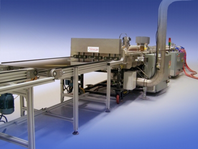
Veeco Instruments Inc. (Nasdaq: VECO), announced the introduction of its FastLine™ platform of Glass Coating Systems, leveraging Veeco's proven PV-Series™ Thermal Deposition Sources. Veeco's new FastLine platform is designed for high throughput, low cost of ownership production of CIGS (copper, indium, gallium and selenium) solar cells.
Veeco Introduces “FastLine” Glass Coating Platform: For Production of CIGS Thin Film Solar Cells
Plainview, NY | Posted on April 27th, 2009Piero Sferlazzo, Ph.D., Senior Vice President of Veeco's Solar Equipment business, commented, "Veeco is now the only equipment company offering integrated production-scale solutions for CIGS manufacturing on glass using thermal evaporation sources for the CIGS/absorber layer. Customers can now choose Veeco to provide comprehensive, fully integrated equipment to manufacture CIGS solar cells, whether they choose to use our FastLine systems for glass or our FastFlex™ systems for flexible substrates."
Thermal evaporation, as compared to other deposition methods, produces the highest efficiency thin film solar cells and has the lowest materials costs with high material utilization driving down the manufacturing cost per watt. Veeco's FastLine systems can handle up to thirty 1.1m x 1.4m glass panels/hour. The modular architecture of the system allows customers to scale their output according to their needs.
The U.S. Department of Energy's National Renewable Energy Laboratory (NREL) has claimed a world record for CIGS thin-film solar cell conversion efficiency of 19.9 percent. The conversion efficiency for CIGS is now close to that of multi-crystalline silicon-based solar cells, according to NREL. This achievement was hailed as an important milestone because the efficiency of thin film solar cells is now achieving its goal of matching silicon in performance.
####
About Veeco Instruments Inc.
Veeco Instruments Inc. manufactures enabling solutions for customers in the HB-LED, solar, data storage, semiconductor, scientific research and industrial markets. We have leading technology positions in our three businesses: LED & Solar Process Equipment, Data Storage Process Equipment, and Metrology Instruments. Veeco’s manufacturing and engineering facilities are located in New York, New Jersey, California, Colorado, Arizona, Massachusetts and Minnesota. Global sales and service offices are located throughout the U.S., Europe, Japan and APAC.
To the extent that this news release discusses expectations or otherwise makes statements about the future, such statements are forward-looking and are subject to a number of risks and uncertainties that could cause actual results to differ materially from the statements made. These factors include the risks discussed in the Business Description and Management's Discussion and Analysis sections of Veeco's Annual Report on Form 10-K for the year ended December 31, 2008 and in our subsequent quarterly reports on Form 10-Q, current reports on Form 8-K and press releases. Veeco does not undertake any obligation to update any forward-looking statements to reflect future events or circumstances after the date of such statements.
For more information, please click here
Contacts:
Investor Contact:
Deb Wasser
SVP
Investor Relations
1-516-677-0200 x 1472
Trade Media Contact:
Fran Brennen
Senior Director of Marcom
1-516-677-0200 x1222
Copyright © Veeco Instruments Inc.
If you have a comment, please Contact us.Issuers of news releases, not 7th Wave, Inc. or Nanotechnology Now, are solely responsible for the accuracy of the content.
Bookmark:


| Related News Press |
News and information
![]() Quantum computer improves AI predictions April 17th, 2026
Quantum computer improves AI predictions April 17th, 2026
![]() Flexible sensor gains sensitivity under pressure April 17th, 2026
Flexible sensor gains sensitivity under pressure April 17th, 2026
![]() A reusable chip for particulate matter sensing April 17th, 2026
A reusable chip for particulate matter sensing April 17th, 2026
![]() Detecting vibrational quantum beating in the predissociation dynamics of SF6 using time-resolved photoelectron spectroscopy April 17th, 2026
Detecting vibrational quantum beating in the predissociation dynamics of SF6 using time-resolved photoelectron spectroscopy April 17th, 2026
Thin films
![]() Tiny nanosheets, big leap: A new sensor detects ethanol at ultra-low levels January 30th, 2026
Tiny nanosheets, big leap: A new sensor detects ethanol at ultra-low levels January 30th, 2026
![]() Utilizing palladium for addressing contact issues of buried oxide thin film transistors April 5th, 2024
Utilizing palladium for addressing contact issues of buried oxide thin film transistors April 5th, 2024
![]() Understanding the mechanism of non-uniform formation of diamond film on tools: Paving the way to a dry process with less environmental impact March 24th, 2023
Understanding the mechanism of non-uniform formation of diamond film on tools: Paving the way to a dry process with less environmental impact March 24th, 2023
![]() New study introduces the best graphite films: The work by Distinguished Professor Feng Ding at UNIST has been published in the October 2022 issue of Nature Nanotechnology November 4th, 2022
New study introduces the best graphite films: The work by Distinguished Professor Feng Ding at UNIST has been published in the October 2022 issue of Nature Nanotechnology November 4th, 2022
Announcements
![]() A fundamentally new therapeutic approach to cystic fibrosis: Nanobody repairs cellular defect April 17th, 2026
A fundamentally new therapeutic approach to cystic fibrosis: Nanobody repairs cellular defect April 17th, 2026
![]() UC Irvine physicists discover method to reverse ‘quantum scrambling’ : The work addresses the problem of information loss in quantum computing system April 17th, 2026
UC Irvine physicists discover method to reverse ‘quantum scrambling’ : The work addresses the problem of information loss in quantum computing system April 17th, 2026
Tools
![]() Metasurfaces smooth light to boost magnetic sensing precision January 30th, 2026
Metasurfaces smooth light to boost magnetic sensing precision January 30th, 2026
![]() From sensors to smart systems: the rise of AI-driven photonic noses January 30th, 2026
From sensors to smart systems: the rise of AI-driven photonic noses January 30th, 2026
![]() Japan launches fully domestically produced quantum computer: Expo visitors to experience quantum computing firsthand August 8th, 2025
Japan launches fully domestically produced quantum computer: Expo visitors to experience quantum computing firsthand August 8th, 2025
Energy
![]() Sensors innovations for smart lithium-based batteries: advancements, opportunities, and potential challenges August 8th, 2025
Sensors innovations for smart lithium-based batteries: advancements, opportunities, and potential challenges August 8th, 2025
![]() Simple algorithm paired with standard imaging tool could predict failure in lithium metal batteries August 8th, 2025
Simple algorithm paired with standard imaging tool could predict failure in lithium metal batteries August 8th, 2025
Solar/Photovoltaic
![]() Spinel-type sulfide semiconductors to operate the next-generation LEDs and solar cells For solar-cell absorbers and green-LED source October 3rd, 2025
Spinel-type sulfide semiconductors to operate the next-generation LEDs and solar cells For solar-cell absorbers and green-LED source October 3rd, 2025
![]() KAIST researchers introduce new and improved, next-generation perovskite solar cell November 8th, 2024
KAIST researchers introduce new and improved, next-generation perovskite solar cell November 8th, 2024
![]() Groundbreaking precision in single-molecule optoelectronics August 16th, 2024
Groundbreaking precision in single-molecule optoelectronics August 16th, 2024
![]() Development of zinc oxide nanopagoda array photoelectrode: photoelectrochemical water-splitting hydrogen production January 12th, 2024
Development of zinc oxide nanopagoda array photoelectrode: photoelectrochemical water-splitting hydrogen production January 12th, 2024
|
|
||
|
|
||
| The latest news from around the world, FREE | ||
|
|
||
|
|
||
| Premium Products | ||
|
|
||
|
Only the news you want to read!
Learn More |
||
|
|
||
|
Full-service, expert consulting
Learn More |
||
|
|
||