Home > Press > New Laser Technique Advances Nanofabrication Process
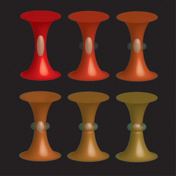 |
| Schematic depictions of RAPID lithography, the technique developed by John Fourkas and colleagues which enables the creation of features 2500 times smaller than the width of a human hair. |
Abstract:
The ability to create tiny patterns is essential to the fabrication of computer chips and many other current and potential applications of nanotechnology. Yet, creating ever smaller features, through a widely-used process called photolithography, has required the use of ultraviolet light, which is difficult and expensive to work with.
New Laser Technique Advances Nanofabrication Process
College Park, MD | Posted on April 10th, 2009John Fourkas, Professor of Chemistry and Biochemistry in the University of Maryland College of Chemical and Life Sciences, and his research group have developed a new, table-top technique called RAPID (Resolution Augmentation through Photo-Induced Deactivation) lithography that makes it possible to create small features without the use of ultraviolet light. This research is to be published in Science magazine and released on Science Express on April 9, 2009.
Photolithography uses light to deposit or remove material and create patterns on a surface. There is usually a direct relationship between the wavelength of light used and the feature size created. Therefore, nanofabrication has depended on short wavelength ultraviolet light to generate ever smaller features.
"The RAPID lithography technique we have developed enables us to create patterns twenty times smaller than the wavelength of light employed,"explains Dr. Fourkas, "which means that it streamlines the nanofabrication process. We expect RAPID to find many applications in areas such as electronics, optics, and biomedical devices."
"If you have gotten a filling at the dentist in recent years,"says Fourkas, "you have seen that a viscous liquid is squirted into the cavity and a blue light is then used to harden it. A similar process of hardening using light is the first element of RAPID. Now imagine that your dentist could use a second light source to sculpt the filling by preventing it from hardening in certain places. We have developed a way of using a second light source to perform this sculpting, and it allows us to create features that are 2500 times smaller than the width of a human hair."
Both of the laser light sources used by Fourkas and his team were of the same color, the only difference being that the laser used to harden the material produced short bursts of light while the laser used to prevent hardening was on constantly. The second laser beam also passed through a special optic that allowed for sculpting of the hardened features in the desired shape.
"The fact that one laser is on constantly in RAPID makes this technique particularly easy to implement,"says Fourkas, "because there is no need to control the timing between two different pulsed lasers."
Fourkas and his team are currently working on improvements to RAPID lithography that they believe will make it possible to create features that are half of the size of the ones they have demonstrated to date.
Achieving lambda/20 Resolution by One-Color Initiation and Deactivation of Polymerization was written by Linjie Li, Rafael R. Gattass, Erez Gershgorem, Hana Hwang and John T. Fourkas.
####
About University of Maryland, College Park
The University of Maryland, College Park (often referred to as The University of Maryland, UMD, UMCP, College Park, or simply Maryland) is a public research university located in the city of College Park in Prince George's County, Maryland outside Washington, D.C. Founded in 1856, the University of Maryland is the flagship institution of the University System of Maryland. The university is considered to be a Public Ivy. At a total enrollment of 36,014 students, Maryland is the largest university in the state as well as the Washington Metropolitan Area. It is a member of the Association of American Universities and a founding member of the Atlantic Coast Conference athletic league.
Source: Wikipedia
Contacts:
Kelly Blake
301-405-8203
Issuers of news releases, not 7th Wave, Inc. or Nanotechnology Now, are solely responsible for the accuracy of the content.
Bookmark:


| Related News Press |
News and information
![]() Quantum computer improves AI predictions April 17th, 2026
Quantum computer improves AI predictions April 17th, 2026
![]() Flexible sensor gains sensitivity under pressure April 17th, 2026
Flexible sensor gains sensitivity under pressure April 17th, 2026
![]() A reusable chip for particulate matter sensing April 17th, 2026
A reusable chip for particulate matter sensing April 17th, 2026
![]() Detecting vibrational quantum beating in the predissociation dynamics of SF6 using time-resolved photoelectron spectroscopy April 17th, 2026
Detecting vibrational quantum beating in the predissociation dynamics of SF6 using time-resolved photoelectron spectroscopy April 17th, 2026
Possible Futures
![]() A fundamentally new therapeutic approach to cystic fibrosis: Nanobody repairs cellular defect April 17th, 2026
A fundamentally new therapeutic approach to cystic fibrosis: Nanobody repairs cellular defect April 17th, 2026
![]() UC Irvine physicists discover method to reverse �quantum scrambling� : The work addresses the problem of information loss in quantum computing system April 17th, 2026
UC Irvine physicists discover method to reverse �quantum scrambling� : The work addresses the problem of information loss in quantum computing system April 17th, 2026
Chip Technology
![]() A reusable chip for particulate matter sensing April 17th, 2026
A reusable chip for particulate matter sensing April 17th, 2026
![]() Metasurfaces smooth light to boost magnetic sensing precision January 30th, 2026
Metasurfaces smooth light to boost magnetic sensing precision January 30th, 2026
Nanoelectronics
![]() Lab to industry: InSe wafer-scale breakthrough for future electronics August 8th, 2025
Lab to industry: InSe wafer-scale breakthrough for future electronics August 8th, 2025
![]() Interdisciplinary: Rice team tackles the future of semiconductors Multiferroics could be the key to ultralow-energy computing October 6th, 2023
Interdisciplinary: Rice team tackles the future of semiconductors Multiferroics could be the key to ultralow-energy computing October 6th, 2023
![]() Key element for a scalable quantum computer: Physicists from Forschungszentrum J�lich and RWTH Aachen University demonstrate electron transport on a quantum chip September 23rd, 2022
Key element for a scalable quantum computer: Physicists from Forschungszentrum J�lich and RWTH Aachen University demonstrate electron transport on a quantum chip September 23rd, 2022
![]() Reduced power consumption in semiconductor devices September 23rd, 2022
Reduced power consumption in semiconductor devices September 23rd, 2022
Announcements
![]() A fundamentally new therapeutic approach to cystic fibrosis: Nanobody repairs cellular defect April 17th, 2026
A fundamentally new therapeutic approach to cystic fibrosis: Nanobody repairs cellular defect April 17th, 2026
![]() UC Irvine physicists discover method to reverse �quantum scrambling� : The work addresses the problem of information loss in quantum computing system April 17th, 2026
UC Irvine physicists discover method to reverse �quantum scrambling� : The work addresses the problem of information loss in quantum computing system April 17th, 2026
Photonics/Optics/Lasers
![]() Metasurfaces smooth light to boost magnetic sensing precision January 30th, 2026
Metasurfaces smooth light to boost magnetic sensing precision January 30th, 2026
![]() From sensors to smart systems: the rise of AI-driven photonic noses January 30th, 2026
From sensors to smart systems: the rise of AI-driven photonic noses January 30th, 2026
|
|
||
|
|
||
| The latest news from around the world, FREE | ||
|
|
||
|
|
||
| Premium Products | ||
|
|
||
|
Only the news you want to read!
Learn More |
||
|
|
||
|
Full-service, expert consulting
Learn More |
||
|
|
||