Home > Press > Self-Cleaning, Low-Reflectivity Surface Could Improve PV Cells
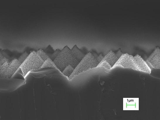 |
| Image shows silicon pyramid structures etched for one minute using a hydrogen fluoride/hydrogen peroxide/water solution. The resulting structure has roughness at the micron and nanometer scales. |
Abstract:
Micron- and Nanometer-Scale Features Make Superhydrophobic Surface
Self-Cleaning, Low-Reflectivity Surface Could Improve PV Cells
Atlanta, GA | Posted on April 8th, 2009Using two different types of chemical etching to create features at both the micron and nanometer size scales, researchers at the Georgia Institute of Technology have developed a surface treatment that could boost the light absorption of silicon photovoltaic cells in two complementary ways.
The surface treatment increases absorption both by trapping light in three-dimensional structures and by making the surfaces self-cleaning - allowing rain or dew to wash away the dust and dirt that can accumulate on photovoltaic arrays. Because of its ability to make water bead up and roll off, the surface is classified as superhydrophobic.
"The more sunlight that goes into the photovoltaic cells and the less that reflects back, the higher the efficiency can be," said C.P. Wong, Regents' professor in Georgia Tech's School of Materials Science and Engineering. "Our simulations show that we can potentially increase the final efficiency of the cells by as much as two percent with this surface structure."
Supported by the National Science Foundation (NSF) and the National Electric Energy Testing Research and Applications Center (NEETRAC) at Georgia Tech, the research was described March 24th at the Spring 2009 National Meeting of the American Chemical Society in Salt Lake City.
The silicon etching treatment mimics the superhydrophobic surface of the lotus leaf, which uses surface roughness at two different size scales to create high contact angles that encourage water from rain or condensation to bead up and run off. As the water runs off, it carries with it any surface dust or dirt - which also doesn't adhere because of the unique surface properties.
In the silicon surface treatment, the two-tier roughness - created with both micron- and nano-scale structures - works in the same way as the lotus leaf, minimizing contact between the water or dust and the surface, Wong noted.
"When a water droplet reaches the surface, it sits on top of this two-tier roughness and only about three percent of it is in contact with the silicon," he explained.
Preparation of the superhydrophobic surface begins with use of a potassium hydroxide (KOH) solution to etch the silicon surface. The solution preferentially removes silicon along crystalline planes, creating micron-scale pyramid structures in the surface.
An e-beam process is then used to apply nanometer-scale gold particles to the pyramid structures. Using a solution of hydrogen fluoride (HF) and hydrogen peroxide (H2O2), a metal-assisted etching process - with gold as the catalyst - produces the nanometer-scale features. The feature size is controlled by the diameter of the gold particles and the length of time the silicon is exposed to the etching.
Finally, the gold is removed with a potassium iodide (KI) solution and the surface coated with a fluorocarbon material, perfluorooctyl tricholosilane (PFOS).
The combination of increased light absorption from the textured surface and the self-cleaning ability both help boost absorption of sunlight hitting the silicon surface.
"A normal silicon surface reflects a lot of the light that comes in, but by doing this texturing, the reflection is reduced to less than five percent," said Dennis Hess, a professor in the Georgia Tech School of Chemical and Biomolecular Engineering. "As much as 10 percent of the light that hits the cells is scattered because of dust and dirt of the surface. If you can keep the cells clean, in principle you can increase the efficiency. Even if you only improve this by a few percent, that could make a big difference."
Even in desert areas where constant sunlight provides ideal conditions for photovoltaic arrays, nighttime dew should provide enough moisture to keep the cells clean, Wong said.
The research team, which also included Yonghao Xiu, Shu Zhang and Yan Liu, is working with Georgia Tech's University Center of Excellence for Photovoltaics Research and Education - headed by Professor Ajeet Rohatgi of the Georgia Tech School of Electrical and Computer Engineering - to evaluate the surface treatment with real solar cells.
However, adoption of the superhydrophobic surface treatment will ultimately depend on its long-term robustness and cost.
"Because the structures are so small, they are fairly fragile," Hess noted. "Mechanical abrasion to the surface can destroy the superhydrophobicity. We have tried to address that here by creating a large superhydrophobic surface area so that small amounts of damage won't affect the overall surface."
Large scale cost estimates haven't yet been done, but Hess said the additional etching and vacuum deposition steps shouldn't add dramatically to the already complex manufacturing process used for fabricating silicon PV cells.
In addition to photovoltaic cells, the surface treatment could be used to create anti-bacterial coatings on medical equipment, micro-electromechanical devices that don't stick together, and improved microfluidic devices.
Writer: John Toon
####
About Georgia Institute of Technology
The Georgia Institute of Technology is one of the nation's premier research universities. Ranked seventh among U.S. News & World Report's top public universities, Georgia Tech's more than 19,000 students are enrolled in its Colleges of Architecture, Computing, Engineering, Liberal Arts, Management and Sciences. Tech is among the nation's top producers of women and African-American engineers. The Institute offers research opportunities to both undergraduate and graduate students and is home to more than 100 interdisciplinary units plus the Georgia Tech Research Institute.
For more information, please click here
Contacts:
Research News & Publications Office
Georgia Institute of Technology
75 Fifth Street, N.W., Suite 100
Atlanta, Georgia 30308 USA
Media Relations Contacts:
John Toon
404-894-6986
or
Abby Vogel
404-385-3364
Technical Contacts: C.P. Wong (404-894-8391); E-mail: or Dennis Hess (404-894-5922); E-mail:
Copyright © Georgia Institute of Technology
If you have a comment, please Contact us.Issuers of news releases, not 7th Wave, Inc. or Nanotechnology Now, are solely responsible for the accuracy of the content.
Bookmark:


| Related News Press |
News and information
![]() Quantum computer improves AI predictions April 17th, 2026
Quantum computer improves AI predictions April 17th, 2026
![]() Flexible sensor gains sensitivity under pressure April 17th, 2026
Flexible sensor gains sensitivity under pressure April 17th, 2026
![]() A reusable chip for particulate matter sensing April 17th, 2026
A reusable chip for particulate matter sensing April 17th, 2026
![]() Detecting vibrational quantum beating in the predissociation dynamics of SF6 using time-resolved photoelectron spectroscopy April 17th, 2026
Detecting vibrational quantum beating in the predissociation dynamics of SF6 using time-resolved photoelectron spectroscopy April 17th, 2026
Chemistry
![]() Projecting light to dispense liquids: A new route to ultra-precise microdroplets January 30th, 2026
Projecting light to dispense liquids: A new route to ultra-precise microdroplets January 30th, 2026
![]() From sensors to smart systems: the rise of AI-driven photonic noses January 30th, 2026
From sensors to smart systems: the rise of AI-driven photonic noses January 30th, 2026
![]() "Nanoreactor" cage uses visible light for catalytic and ultra-selective cross-cycloadditions October 3rd, 2025
"Nanoreactor" cage uses visible light for catalytic and ultra-selective cross-cycloadditions October 3rd, 2025
![]() Cambridge chemists discover simple way to build bigger molecules � one carbon at a time June 6th, 2025
Cambridge chemists discover simple way to build bigger molecules � one carbon at a time June 6th, 2025
Possible Futures
![]() A fundamentally new therapeutic approach to cystic fibrosis: Nanobody repairs cellular defect April 17th, 2026
A fundamentally new therapeutic approach to cystic fibrosis: Nanobody repairs cellular defect April 17th, 2026
![]() UC Irvine physicists discover method to reverse �quantum scrambling� : The work addresses the problem of information loss in quantum computing system April 17th, 2026
UC Irvine physicists discover method to reverse �quantum scrambling� : The work addresses the problem of information loss in quantum computing system April 17th, 2026
Nanomedicine
![]() A fundamentally new therapeutic approach to cystic fibrosis: Nanobody repairs cellular defect April 17th, 2026
A fundamentally new therapeutic approach to cystic fibrosis: Nanobody repairs cellular defect April 17th, 2026
![]() New molecular technology targets tumors and simultaneously silences two �undruggable� cancer genes August 8th, 2025
New molecular technology targets tumors and simultaneously silences two �undruggable� cancer genes August 8th, 2025
![]() New imaging approach transforms study of bacterial biofilms August 8th, 2025
New imaging approach transforms study of bacterial biofilms August 8th, 2025
![]() Electrifying results shed light on graphene foam as a potential material for lab grown cartilage June 6th, 2025
Electrifying results shed light on graphene foam as a potential material for lab grown cartilage June 6th, 2025
Nanoelectronics
![]() Lab to industry: InSe wafer-scale breakthrough for future electronics August 8th, 2025
Lab to industry: InSe wafer-scale breakthrough for future electronics August 8th, 2025
![]() Interdisciplinary: Rice team tackles the future of semiconductors Multiferroics could be the key to ultralow-energy computing October 6th, 2023
Interdisciplinary: Rice team tackles the future of semiconductors Multiferroics could be the key to ultralow-energy computing October 6th, 2023
![]() Key element for a scalable quantum computer: Physicists from Forschungszentrum J�lich and RWTH Aachen University demonstrate electron transport on a quantum chip September 23rd, 2022
Key element for a scalable quantum computer: Physicists from Forschungszentrum J�lich and RWTH Aachen University demonstrate electron transport on a quantum chip September 23rd, 2022
![]() Reduced power consumption in semiconductor devices September 23rd, 2022
Reduced power consumption in semiconductor devices September 23rd, 2022
Announcements
![]() A fundamentally new therapeutic approach to cystic fibrosis: Nanobody repairs cellular defect April 17th, 2026
A fundamentally new therapeutic approach to cystic fibrosis: Nanobody repairs cellular defect April 17th, 2026
![]() UC Irvine physicists discover method to reverse �quantum scrambling� : The work addresses the problem of information loss in quantum computing system April 17th, 2026
UC Irvine physicists discover method to reverse �quantum scrambling� : The work addresses the problem of information loss in quantum computing system April 17th, 2026
Solar/Photovoltaic
![]() Spinel-type sulfide semiconductors to operate the next-generation LEDs and solar cells For solar-cell absorbers and green-LED source October 3rd, 2025
Spinel-type sulfide semiconductors to operate the next-generation LEDs and solar cells For solar-cell absorbers and green-LED source October 3rd, 2025
![]() KAIST researchers introduce new and improved, next-generation perovskite solar cell November 8th, 2024
KAIST researchers introduce new and improved, next-generation perovskite solar cell November 8th, 2024
![]() Groundbreaking precision in single-molecule optoelectronics August 16th, 2024
Groundbreaking precision in single-molecule optoelectronics August 16th, 2024
![]() Development of zinc oxide nanopagoda array photoelectrode: photoelectrochemical water-splitting hydrogen production January 12th, 2024
Development of zinc oxide nanopagoda array photoelectrode: photoelectrochemical water-splitting hydrogen production January 12th, 2024
|
|
||
|
|
||
| The latest news from around the world, FREE | ||
|
|
||
|
|
||
| Premium Products | ||
|
|
||
|
Only the news you want to read!
Learn More |
||
|
|
||
|
Full-service, expert consulting
Learn More |
||
|
|
||