Home > Press > Nano-structured parts
 |
Abstract:
Materials with a nanoparticle structure are stronger and harder than materials made of larger particles. A new manufacturing technique ensures that such microcrystalline structures remain intact when being processed.
Nano-structured parts
Germany | Posted on February 3rd, 2009
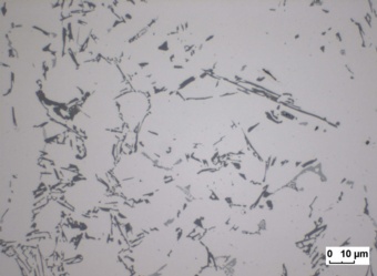
Aluminum is light but also bends easily. However, if it has a nanometer structure, it features quite different properties: The material is much stronger and firmer, and this makes it ideal for engine screws, which have to withstand high temperatures. It is also eminently suitable for making lightweight parts, for the stronger the material, the thinner the sheets for the components can be made. The material's properties are mainly due to the tiny size of its crystals. These are much smaller than those in conventional materials, hence the designation "microcrystalline structures".
One of the challenges posed by such nano materials lies in processing them to make tools or components. Pressing or joining requires that the material be heated. This causes the crystals to grow, so the structures become larger. In short, the material loses its "nano properties" as it heats up. Researchers at the Fraunhofer Institute for Manufacturing Engineering and Applied Materials Research IFAM in Dresden have risen to the challenge. "Our goal is to preserve the material's microcrystalline structure throughout the entire component manufacturing process," states IFAM project manager Dr. Ronny Leuschner. To this end, the researchers have set up a special technology chain for manufacturing nano-structured aluminum and other materials. "First of all, we produce a special aluminum alloy," says Leuschner. "The metal melt has to be cooled very rapidly, so we virtually freeze it." This is done using the "melt spinning" technique: A specially developed spraying device pours the melt onto a water-cooled rotating roller, producing uniform strips or "flakes" no more than a few micrometers thick. As soon as it hits the roller, the melt rapidly loses heat and the flakes solidify at top speed. The advantage of this system is that it can handle several kilograms of material and withstand temperatures of more than 1700 degrees Celsius. "Once they have solidified, the flakes need to be compacted and pressed into the desired shape," explains Leuschner. During this step, too, their microcrystalline structures must remain intact. The method the researchers use in this case is spark plasma sintering: High-frequency current pulses inside the press compact the material in a very short space of time so that the fine microstructures are preserved. Applications for these nano materials range from lightweight aluminum parts with greater strength and improved wear and corrosion resistance, to hydrogen storage, energy production with thermoelectric materials, and electrical engineering.
####
For more information, please click here
Contacts:
Dr.-Ing. Ronny Leuschner
Phone: +49 351 2537-397
Fax: +49 351 2554-492
Fraunhofer Institute for Manufacturing Technology and Applied Materials Research
IFAM-DD
Winterbergstr. 28
01277 Dresden
Copyright © Fraunhofer-Gesellschaft
If you have a comment, please Contact us.Issuers of news releases, not 7th Wave, Inc. or Nanotechnology Now, are solely responsible for the accuracy of the content.
Bookmark:


| Related News Press |
News and information
![]() Simulating magnetization in a Heisenberg quantum spin chain April 5th, 2024
Simulating magnetization in a Heisenberg quantum spin chain April 5th, 2024
![]() NRL charters Navy�s quantum inertial navigation path to reduce drift April 5th, 2024
NRL charters Navy�s quantum inertial navigation path to reduce drift April 5th, 2024
![]() Discovery points path to flash-like memory for storing qubits: Rice find could hasten development of nonvolatile quantum memory April 5th, 2024
Discovery points path to flash-like memory for storing qubits: Rice find could hasten development of nonvolatile quantum memory April 5th, 2024
Discoveries
![]() Chemical reactions can scramble quantum information as well as black holes April 5th, 2024
Chemical reactions can scramble quantum information as well as black holes April 5th, 2024
![]() New micromaterial releases nanoparticles that selectively destroy cancer cells April 5th, 2024
New micromaterial releases nanoparticles that selectively destroy cancer cells April 5th, 2024
![]() Utilizing palladium for addressing contact issues of buried oxide thin film transistors April 5th, 2024
Utilizing palladium for addressing contact issues of buried oxide thin film transistors April 5th, 2024
Materials/Metamaterials/Magnetoresistance
![]() Nanoscale CL thermometry with lanthanide-doped heavy-metal oxide in TEM March 8th, 2024
Nanoscale CL thermometry with lanthanide-doped heavy-metal oxide in TEM March 8th, 2024
![]() Focused ion beam technology: A single tool for a wide range of applications January 12th, 2024
Focused ion beam technology: A single tool for a wide range of applications January 12th, 2024
Announcements
![]() NRL charters Navy�s quantum inertial navigation path to reduce drift April 5th, 2024
NRL charters Navy�s quantum inertial navigation path to reduce drift April 5th, 2024
![]() Discovery points path to flash-like memory for storing qubits: Rice find could hasten development of nonvolatile quantum memory April 5th, 2024
Discovery points path to flash-like memory for storing qubits: Rice find could hasten development of nonvolatile quantum memory April 5th, 2024
Energy
![]() Development of zinc oxide nanopagoda array photoelectrode: photoelectrochemical water-splitting hydrogen production January 12th, 2024
Development of zinc oxide nanopagoda array photoelectrode: photoelectrochemical water-splitting hydrogen production January 12th, 2024
![]() Shedding light on unique conduction mechanisms in a new type of perovskite oxide November 17th, 2023
Shedding light on unique conduction mechanisms in a new type of perovskite oxide November 17th, 2023
![]() Inverted perovskite solar cell breaks 25% efficiency record: Researchers improve cell efficiency using a combination of molecules to address different November 17th, 2023
Inverted perovskite solar cell breaks 25% efficiency record: Researchers improve cell efficiency using a combination of molecules to address different November 17th, 2023
![]() The efficient perovskite cells with a structured anti-reflective layer � another step towards commercialization on a wider scale October 6th, 2023
The efficient perovskite cells with a structured anti-reflective layer � another step towards commercialization on a wider scale October 6th, 2023
|
|
||
|
|
||
| The latest news from around the world, FREE | ||
|
|
||
|
|
||
| Premium Products | ||
|
|
||
|
Only the news you want to read!
Learn More |
||
|
|
||
|
Full-service, expert consulting
Learn More |
||
|
|
||