Home > Press > Applied Materials' New SEMVision G4 System Sets the Benchmark with Defect-Per-Second Review at 2nm Resolution
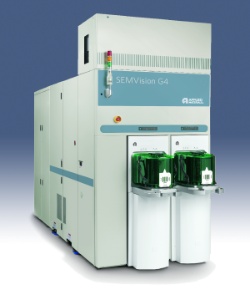 |
| Applied Materials' SEMVision G4 sets new standards for image quality and productivity while adding new technologies to accelerate defect root cause analysis and boost yield in volume manufacturing. (Photo: Business Wire) |
Abstract:
Applied Materials, Inc. today unveiled its most advanced defect review SEM1, the Applied SEMVision™ G4, which extends the technology and productivity of Applied's highly successful SEMVision system to 45 nm and beyond applications. Key to the SEMVision G4 are its new SEM column technology and enhanced multi-perspective SEM imaging system (MPSI) that deliver state-of-the-art 2nm physical resolution for unmatched image quality at a benchmark one defect-per-second review rate.
Applied Materials' New SEMVision G4 System Sets the Benchmark with Defect-Per-Second Review at 2nm Resolution
SANTA CLARA, CA | Posted on December 5th, 2007 "The task of reliable and high productivity defect review and classification at 45nm in high-aspect ratio and densely packed memory and logic structures requires unprecedented SEM performance," said Ronen Benzion, general manager of the SEM division of Applied Materials' Process Diagnostics and Control business unit. "The SEMVision G4 sets new standards for image quality and productivity while adding new technologies that allow customers to accelerate defect root cause analysis and boost yield."
"The SEMVision G4 has recently been put into production and is expected to have a significant role in our in-line defect root cause analysis strategy," said Tomoharu Watanabe, senior manager of Yokkaichi Operations Manufacturing Engineering Department, Semiconductor Company, Toshiba Corporation.
The SEMVision G4 brings several advanced defect monitoring capabilities from the engineering floor to in-line volume manufacturing. These vital analytical tools enable customers to rapidly analyze and classify defects as small as 30nm in the most sensitive device layers, such as immersion photoresist and low-k dielectrics. Featuring EDXtreme, a revolution in EDX1-based material analysis, the SEMVision G4 extends the chemical characterization of defects to sub-50nm particle sizes. The system's new SEM column can rotate and tilt up to 45° relative to the wafer to provide complete 3-D data for superior defect visualization and classification. In addition, wafer edge and bevel analysis technology address a new frontier of yield enhancement, enabling customers to successfully address immersion-related defectivity issues.
Additional information on the SEMVision G4 will be presented at Applied Materials' booth #3D-1001 at SEMICON Japan, taking place on December 5-7, 2007 in Chiba, as part of Applied's integrated 45nm portfolio. Also, please visit http://www.appliedmaterials.com/products/semvision_g4_4.html .
1 SEM=scanning electron microscope
EDX = Energy-dispersive X-ray spectroscopy
####
About Applied Materials, Inc.
Applied Materials, Inc. (Nasdaq:AMAT) is the global leader in Nanomanufacturing Technology™ solutions with a broad portfolio of innovative equipment, service and software products for the fabrication of semiconductor chips, flat panel displays, solar photovoltaic cells, flexible electronics and energy efficient glass. At Applied Materials, we apply Nanomanufacturing Technology to improve the way people live.
For more information, please click here
Contacts:
Applied Materials, Inc.
Betty Newboe
408-563-0647 (editorial/media)
Randy Bane
408-986-7977 (financial community)
Copyright © Business Wire 2007
If you have a comment, please Contact us.Issuers of news releases, not 7th Wave, Inc. or Nanotechnology Now, are solely responsible for the accuracy of the content.
Bookmark:


| Related News Press |
Announcements
![]() NRL charters Navy’s quantum inertial navigation path to reduce drift April 5th, 2024
NRL charters Navy’s quantum inertial navigation path to reduce drift April 5th, 2024
![]() Discovery points path to flash-like memory for storing qubits: Rice find could hasten development of nonvolatile quantum memory April 5th, 2024
Discovery points path to flash-like memory for storing qubits: Rice find could hasten development of nonvolatile quantum memory April 5th, 2024
Tools
![]() Ferroelectrically modulate the Fermi level of graphene oxide to enhance SERS response November 3rd, 2023
Ferroelectrically modulate the Fermi level of graphene oxide to enhance SERS response November 3rd, 2023
![]() The USTC realizes In situ electron paramagnetic resonance spectroscopy using single nanodiamond sensors November 3rd, 2023
The USTC realizes In situ electron paramagnetic resonance spectroscopy using single nanodiamond sensors November 3rd, 2023
Events/Classes
![]() Researchers demonstrate co-propagation of quantum and classical signals: Study shows that quantum encryption can be implemented in existing fiber networks January 20th, 2023
Researchers demonstrate co-propagation of quantum and classical signals: Study shows that quantum encryption can be implemented in existing fiber networks January 20th, 2023
|
|
||
|
|
||
| The latest news from around the world, FREE | ||
|
|
||
|
|
||
| Premium Products | ||
|
|
||
|
Only the news you want to read!
Learn More |
||
|
|
||
|
Full-service, expert consulting
Learn More |
||
|
|
||