Home > Press > New Microprinting Technique Improves Nanoscale Fabrication
Abstract:
Microdisplacement printing makes possible highly precise placement of molecules during the fabrication of nanoscale components
New Microprinting Technique Improves Nanoscale Fabrication
August 18, 2005
Scientists will announce next month a new technique called microdisplacement printing, which makes possible the highly precise placement of molecules during the fabrication of nanoscale components for electronic and sensing devices. The new technique, which also extends the library of molecules that can be used for patterning, will be described in the 14 September issue of the journal Nano Letters by a team led by Paul S. Weiss, professor of chemistry and physics at Penn State.
The new microdisplacement technique is based on a widely used patterning method known as microcontact printing -- a simple way of fabricating chemical patterns that does not require clean rooms and other kinds of special and expensive environments. Both methods involve "inking" a patterned rubber-like stamp with a solution of molecules, then applying the inked stamp to a surface.
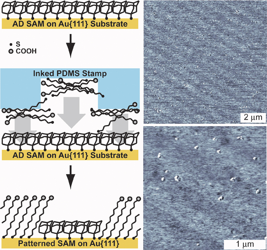
A demonstration of microdisplacement printing, in which a weakly bound film is displaced by contact stamping with molecules that bind more strongly to the substrate. This process leaves a patterned film with regions of strongly bound molecules (where the weakly bound molecules were displaced) and regions of the remaining weakly bound molecules.
|
"Microdisplacement gives us more control over the precision with which the patterns are placed and retained, and also allows us to use a wider range of molecules," Weiss says.
One of the limitations of microcontact printing is that its precision is limited at the edges of a stamped pattern by the tendency of the applied molecules to skitter across the stamped surface, blurring or obliterating the applied pattern and destroying its usefulness. Weiss's improved microdisplacement technique solves this problem by applying a self-assembled-monolayer film -- a single ordered layer of spherical adamantanethiolate molecules -- to keep the stamped molecules in place on the surface. "We specifically engineered the adamantanethiol molecule to have a very weak chemical bond with the surface so that it would detach easily when bumped by a stronger-bonding molecule," Weiss explains. The molecules inked on the stamp replace the adamantanethiolate molecules wherever they touch the monolayer film, but the surrounding molecules in the film remain attached to the surface to prevent the applied molecules from wandering.
"Microdisplacement printing uses many of the same procedures as microcontact printing except one first prepares the substrate by coating it with a self-assembled monolayer of adamantanethiolate, which is inexpensive and easy to apply," Weiss explains. "You dip the substrate in a solution of these molecules, pull it out, and they assemble themselves into an ordered film one molecule thick."
In addition to providing more control over the precision of stamped patterns, the new microdisplacement technique also relaxes the requirements in precisely positioning a series of stamps used to apply consecutive patterns with different molecular inks. "You don't have to be extremely precise about the exact placement of the stamps as long as you apply the molecular inks in order of their bonding strengths," Weiss explains. Each successive layer of molecules either will displace or will not displace the already-applied molecules, depending on their relative bonding strengths with the underlying surface.
The research was aided by the Weiss lab's unusual collection of microscopes, which enable the scientists to get a clear picture of the results of their experiments, both at the broad scale of a stamped pattern and at the narrow scale of just a single molecule. One scanning tunneling microscope that Weiss and his group designed and built themselves, for example, has 1,000 times more resolution than is needed to image an individual atom.
Adamantanethiol is related to the family of alkanethiol molecules, which have been studied extensively as a model systems for their ability to form well-ordered monolayer films on gold. Weiss and his team were studying the adamantanethiolate-on-gold system when graduate student Arrelaine Dameron discovered that stronger-bonding molecules easily displaced the adamantanethiolate molecules. Her discovery has led to further studies of this system by the Weiss team, including how the displacement can be applied in a broad range of applications using a variety of materials.
"We have mapped out strategies in this model system and are now investigating how we can apply these strategies more broadly as the chemistry is developed for self-assembled monolayers on other substrates, especially semiconductors," Weiss says. "Our goals are to see how far we can take these kinds of simple techniques, along with our knowledge of intermolecular interactions, to bridge the 1-to-100-nanometer length scale in nanofabrication, which even at the high end currently requires very difficult, slow, and expensive techniques."
In addition to Weiss and Dameron, the Penn State research team includes postdoctoral fellows Jennifer Hampton and Susan Gillmor and graduate students Rachel Smith and T. J. Mullen. The research was supported by the Air Force Office of Scientific Research, the Army Research Office, the Defense Advanced Research Projects Agency, the National Science Foundation, the Office of Naval Research, and the Semiconductor Research Corporation. The work was performed as a part of both the Center for Nanoscale Science and the National Nanofabrication Infrastructure Network.
Paul Weiss
stm@psu.edu
(+1) 814-865-3693
Barbara Kennedy (PIO)
science@psu.edu
(+1) 814-863-4682
Copyright � Penn State
If you have a comment, please Contact us.
Issuers of news releases, not 7th Wave, Inc. or Nanotechnology Now, are solely responsible for the accuracy of the content.
Bookmark:


| Related News Press |
Self Assembly
![]() Diamond glitter: A play of colors with artificial DNA crystals May 17th, 2024
Diamond glitter: A play of colors with artificial DNA crystals May 17th, 2024
![]() Liquid crystal templated chiral nanomaterials October 14th, 2022
Liquid crystal templated chiral nanomaterials October 14th, 2022
![]() Nanoclusters self-organize into centimeter-scale hierarchical assemblies April 22nd, 2022
Nanoclusters self-organize into centimeter-scale hierarchical assemblies April 22nd, 2022
![]() Atom by atom: building precise smaller nanoparticles with templates March 4th, 2022
Atom by atom: building precise smaller nanoparticles with templates March 4th, 2022
Sensors
![]() Flexible sensor gains sensitivity under pressure April 17th, 2026
Flexible sensor gains sensitivity under pressure April 17th, 2026
![]() Tiny nanosheets, big leap: A new sensor detects ethanol at ultra-low levels January 30th, 2026
Tiny nanosheets, big leap: A new sensor detects ethanol at ultra-low levels January 30th, 2026
![]() From sensors to smart systems: the rise of AI-driven photonic noses January 30th, 2026
From sensors to smart systems: the rise of AI-driven photonic noses January 30th, 2026
![]() Sensors innovations for smart lithium-based batteries: advancements, opportunities, and potential challenges August 8th, 2025
Sensors innovations for smart lithium-based batteries: advancements, opportunities, and potential challenges August 8th, 2025
Materials/Metamaterials/Magnetoresistance
![]() First real-time observation of two-dimensional melting process: Researchers at Mainz University unveil new insights into magnetic vortex structures August 8th, 2025
First real-time observation of two-dimensional melting process: Researchers at Mainz University unveil new insights into magnetic vortex structures August 8th, 2025
![]() Researchers unveil a groundbreaking clay-based solution to capture carbon dioxide and combat climate change June 6th, 2025
Researchers unveil a groundbreaking clay-based solution to capture carbon dioxide and combat climate change June 6th, 2025
![]() A 1960s idea inspires NBI researchers to study hitherto inaccessible quantum states June 6th, 2025
A 1960s idea inspires NBI researchers to study hitherto inaccessible quantum states June 6th, 2025
![]() Institute for Nanoscience hosts annual proposal planning meeting May 16th, 2025
Institute for Nanoscience hosts annual proposal planning meeting May 16th, 2025
Announcements
![]() A fundamentally new therapeutic approach to cystic fibrosis: Nanobody repairs cellular defect April 17th, 2026
A fundamentally new therapeutic approach to cystic fibrosis: Nanobody repairs cellular defect April 17th, 2026
![]() UC Irvine physicists discover method to reverse �quantum scrambling� : The work addresses the problem of information loss in quantum computing system April 17th, 2026
UC Irvine physicists discover method to reverse �quantum scrambling� : The work addresses the problem of information loss in quantum computing system April 17th, 2026
|
|
||
|
|
||
| The latest news from around the world, FREE | ||
|
|
||
|
|
||
| Premium Products | ||
|
|
||
|
Only the news you want to read!
Learn More |
||
|
|
||
|
Full-service, expert consulting
Learn More |
||
|
|
||