Home > Press > Penn Researchers Take a Big Step Forward in Making Smaller Circuits
Abstract:
Nanotubes used to create a functional electronic circuit
Penn Researchers Take a Big Step Forward in Making Smaller Circuits
Philadelphia, PA | July 29, 2005
Physicists at the University of Pennsylvania have overcome a major hurdle in the race to create nanotube-based electronics. In an article in the August issue of the journal Nature Materials, available online now, the researchers describe their method of using nanotubes - tiny tubes entirely composed of carbon atoms - to create a functional electronic circuit. Their method creates circuits by dipping semiconductor chips into liquid suspensions of carbon nanotubes, rather than growing the nanotubes directly on the circuit.
"Given their amazing electric properties, nanotubes have been a subject of keen interest for creating such things as chemical sensors, flexible electronics and high-speed, high-device-density microprocessors for computing," said Alan T. Johnson, associate professor in Penn's Department of Physics and Astronomy. "The problem is that the properties we like best about nanotubes their size and physical properties also make them very difficult to manipulate."
Instead of growing nanotubes in a pattern on a silicon chip, as is conventionally done, the Penn researchers devised a means of "sprinkling" nanotubes onto chips.
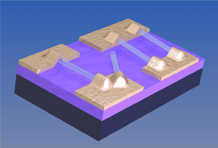
An image showing a circuit made of nanotubes. Copyright © University of Pennsylvania
|
"We dip the chips into nanotubes much like dipping an ice cream cone into candy," said Danvers Johnston, a graduate student in Johnson's laboratory and lead author of the study. "Ultimately we can make it so that the nanotubes only stick where want them to in order to form a circuit."
Single-walled nanotubes are formed by turning a single sheet of carbon atoms into a seamless cylinder approximately one nanometer a billionth of a meter in diameter.
Nanotubes can be either semiconducting or "metallic" the latter is highly conductive to electricity depending on the exact geometry of the carbon atoms. Semiconducting nanotubes make for exceptional transistors, which is why so much attention has been devoted to finding a way to use them in electronics.
Previously, most nanotube circuits have been made by growing each nanotube on the surface of a chip, using a process known as chemical vapor deposition. Unfortunately, this method often results in a circuit comprised of both types of nanotubes, metallic and semiconducting. Furthermore, the growth direction of the nanotube is arbitrary, and their diameters are large. Small diameter carbon nanotubes are more useful for switches.
"Fortunately, other researchers have made it possible to grow small diameter nanotubes and to separate metallic from semiconducting nanotubes in solution," said Arjun Yodh, a professor in Penn's Department of Physics and Astronomy. "Ultimately our process can create a large batch of small diameter nanotubes in solution, can separate out the semiconducting nanotubes and then can place them in proper position on a patterned silicon chip."
The researchers, along with post-doctoral associate Mohammed F. Islam, found their biggest challenge in purifying the mass-produced nanotubes. The process they used to create nanotubes in bulk frequently adds impurities usually stray bits of carbon and leftover catalysts that ultimately detract from the quality of the nanotubes.
The Penn researchers found a purification scheme for the nanotubes by heating them in moist air with a gentle acid treatment and then using magnetic fields to separate the nanotubes from the impurities. They deposit the nanotubes by dipping a chip covered with a glue-like substance into the nanotube solution, and then they wash off the excess glue and whatever solvents that remain.
The resulting circuits take advantage of unique electrical properties of nanotubes and can be produced in bulk. Since the researchers can create nanotubes via processes separate from the chips, this process allows for a better control of the quality and diameter. The Penn researchers believe there is a definite role for nanotechnology in the future of electronics.
"The only way to make faster processors is to cram more transistors together," Johnson said. "Nanotubes are just about the smallest transistors that exist right now. So the more densely they can be packed on a chip, the faster the chips can become."
Funding for this research was provided by grants from the National Science Foundation and NASA.
Contact:
Greg Lester
215-898-8721
glester@pobox.upenn.edu
Copyright � University of Pennsylvania
If you have a comment, please Contact us.
Issuers of news releases, not 7th Wave, Inc. or Nanotechnology Now, are solely responsible for the accuracy of the content.
Bookmark:


| Related News Press |
Possible Futures
![]() A fundamentally new therapeutic approach to cystic fibrosis: Nanobody repairs cellular defect April 17th, 2026
A fundamentally new therapeutic approach to cystic fibrosis: Nanobody repairs cellular defect April 17th, 2026
![]() UC Irvine physicists discover method to reverse �quantum scrambling� : The work addresses the problem of information loss in quantum computing system April 17th, 2026
UC Irvine physicists discover method to reverse �quantum scrambling� : The work addresses the problem of information loss in quantum computing system April 17th, 2026
Chip Technology
![]() A reusable chip for particulate matter sensing April 17th, 2026
A reusable chip for particulate matter sensing April 17th, 2026
![]() Metasurfaces smooth light to boost magnetic sensing precision January 30th, 2026
Metasurfaces smooth light to boost magnetic sensing precision January 30th, 2026
Nanotubes/Buckyballs/Fullerenes/Nanorods/Nanostrings/Nanosheets
![]() Tiny nanosheets, big leap: A new sensor detects ethanol at ultra-low levels January 30th, 2026
Tiny nanosheets, big leap: A new sensor detects ethanol at ultra-low levels January 30th, 2026
![]() Enhancing power factor of p- and n-type single-walled carbon nanotubes April 25th, 2025
Enhancing power factor of p- and n-type single-walled carbon nanotubes April 25th, 2025
![]() Chainmail-like material could be the future of armor: First 2D mechanically interlocked polymer exhibits exceptional flexibility and strength January 17th, 2025
Chainmail-like material could be the future of armor: First 2D mechanically interlocked polymer exhibits exceptional flexibility and strength January 17th, 2025
![]() Innovative biomimetic superhydrophobic coating combines repair and buffering properties for superior anti-erosion December 13th, 2024
Innovative biomimetic superhydrophobic coating combines repair and buffering properties for superior anti-erosion December 13th, 2024
Nanoelectronics
![]() Lab to industry: InSe wafer-scale breakthrough for future electronics August 8th, 2025
Lab to industry: InSe wafer-scale breakthrough for future electronics August 8th, 2025
![]() Interdisciplinary: Rice team tackles the future of semiconductors Multiferroics could be the key to ultralow-energy computing October 6th, 2023
Interdisciplinary: Rice team tackles the future of semiconductors Multiferroics could be the key to ultralow-energy computing October 6th, 2023
![]() Key element for a scalable quantum computer: Physicists from Forschungszentrum J�lich and RWTH Aachen University demonstrate electron transport on a quantum chip September 23rd, 2022
Key element for a scalable quantum computer: Physicists from Forschungszentrum J�lich and RWTH Aachen University demonstrate electron transport on a quantum chip September 23rd, 2022
![]() Reduced power consumption in semiconductor devices September 23rd, 2022
Reduced power consumption in semiconductor devices September 23rd, 2022
Announcements
![]() A fundamentally new therapeutic approach to cystic fibrosis: Nanobody repairs cellular defect April 17th, 2026
A fundamentally new therapeutic approach to cystic fibrosis: Nanobody repairs cellular defect April 17th, 2026
![]() UC Irvine physicists discover method to reverse �quantum scrambling� : The work addresses the problem of information loss in quantum computing system April 17th, 2026
UC Irvine physicists discover method to reverse �quantum scrambling� : The work addresses the problem of information loss in quantum computing system April 17th, 2026
|
|
||
|
|
||
| The latest news from around the world, FREE | ||
|
|
||
|
|
||
| Premium Products | ||
|
|
||
|
Only the news you want to read!
Learn More |
||
|
|
||
|
Full-service, expert consulting
Learn More |
||
|
|
||