Home > Press > Preventing Failure: New Magnetic Testing Technique Helps Ensure Reliability of Microelectronic Devices, PV Cells and MEMS Applications
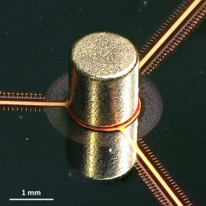 |
| Image shows an assembled magnetically actuated peel test (MAPT) specimen being prepared for analysis at the Georgia Institute of Technology. The silver cylinder in the center is the permanent magnet. (Image courtesy of Greg Ostrowicki and Suresh Sitaraman) |
Abstract:
Taking advantage of the force generated by magnetic repulsion, researchers have developed a new technique for measuring the adhesion strength between thin films of materials used in microelectronic devices, photovoltaic cells and microelectromechanical systems (MEMS).
Preventing Failure: New Magnetic Testing Technique Helps Ensure Reliability of Microelectronic Devices, PV Cells and MEMS Applications
Atlanta, GA | Posted on April 15th, 2012The fixtureless and noncontact technique, known as the magnetically actuated peel test (MAPT), could help ensure the long-term reliability of electronic devices, and assist designers in improving resistance to thermal and mechanical stresses.
"Devices are becoming smaller and smaller, and we are driving them to higher and higher performance," said Suresh Sitaraman, a professor in the George W. Woodruff School of Mechanical Engineering at the Georgia Institute of Technology. "This technique would help manufacturers know that their products will meet reliability requirements, and provide designers with the information they need to choose the right materials to meet future design specifications over the lifetimes of devices."
The research has been supported by the National Science Foundation, and was reported in the March 30, 2012 issue of the journal Thin Solid Films.
Modern microelectronic chips are fabricated from layers of different materials - insulators and conductors - applied on top of one another. Thermal stress can be created when heat generated during the operation of the devices causes the materials of adjacent layers to expand, which occurs at different rates in different materials. The stress can cause the layers to separate, a process known as delamination or de-bonding, which is a major cause of microelectronics failure.
"We need to find out if these layers will separate over time as they are used and subjected to thermal and other stresses," Sitaraman explained. "These systems are used in a wide range of applications from cell phones and computers to automobiles, aircraft and medical equipment. They must be reliable over the course of their expected lifetimes."
Sitaraman and doctoral student Gregory Ostrowicki have used their technique to measure the adhesion strength between layers of copper conductor and silicon dioxide insulator. They also plan to use it to study fatigue cycling failure, which occurs over time as the interface between layers is repeatedly placed under stress. The technique may also be used to study adhesion between layers in photovoltaic systems and in MEMS devices.
The Georgia Tech researchers first used standard microelectronic fabrication techniques to grow layers of thin films that they want to evaluate on a silicon wafer. At the center of each sample, they bonded a tiny permanent magnet made of nickel-plated neodymium (NdFeB), connected to three ribbons of thin-film copper grown atop silicon dioxide on a silicon wafer.
The sample was then placed into a test station that consists of an electromagnet below the sample and an optical profiler above it. Voltage supplied to the electromagnet was increased over time, creating a repulsive force between the like magnetic poles. Pulled upward by the repulsive force on the permanent magnet, the copper ribbons stretched until they finally delaminated.
With data from the optical profiler and knowledge of the magnetic field strength, the researchers can provide an accurate measure of the force required to delaminate the sample. The magnetic actuation has the advantage of providing easily controlled force consistently perpendicular to the silicon wafer.
Because many samples can be made at the same time on the same wafer, the technique can be used to generate a large volume of adhesion data in a timely fashion.
But device failure often occurs gradually over time as the layers are subjected to the stresses of repeated heating and cooling cycles. To study this fatigue failure, Sitaraman and Ostrowicki plan to cycle the electromagnet's voltage on and off.
"A lot of times, layers do not delaminate in one shot," Sitaraman said. "We can test the interface over hundreds or thousands of cycles to see how long it will take to delaminate and for that delamination damage to grow."
The test station is small enough to fit into an environmental chamber, allowing the researchers to evaluate the effects of high temperature and/or high humidity on the strength of the thin film adhesion. This is particularly useful for electronics intended for harsh conditions, such as automobile engine control systems or aircraft avionics, Sitaraman said.
"We can see how the adhesion strength changes or the interfacial fracture toughness varies with temperature and humidity for a wide range of materials," he explained.
So far, Sitaraman and Ostrowicki have studied thin film layers about one micron in thickness, but say their technique will work on layers that are of sub-micron thickness. Because their test layers are made using standard microelectronic fabrication techniques in Georgia Tech's clean rooms, Sitaraman believes they accurately represent the conditions of real devices.
"To get meaningful results, you need to have representative processes and representative materials and representative interfaces so that what is measured is what a real application would face," he said. "We mimic the processing conditions and techniques that are used in actual microelectronics fabrication."
As device sizes continue to decline, Sitaraman says the interfacial issues will grow more important.
"As we continue to scale down the transistor sizes in microelectronics, the layers will get thinner and thinner," he said. "Getting to the nitty-gritty detail of adhesion strength for these layers is where the challenge is. This technique opens up new avenues."
Writer: John Toon
####
For more information, please click here
Contacts:
Research News & Publications Office
Georgia Institute of Technology
75 Fifth Street, N.W., Suite 314
Atlanta, Georgia 30308 USA
Media Relations Contacts:
John Toon
404-894-6986
Abby Robinson
404-894-6986
Copyright © Georgia Tech
If you have a comment, please Contact us.Issuers of news releases, not 7th Wave, Inc. or Nanotechnology Now, are solely responsible for the accuracy of the content.
Bookmark:


| Related News Press |
News and information
![]() Simulating magnetization in a Heisenberg quantum spin chain April 5th, 2024
Simulating magnetization in a Heisenberg quantum spin chain April 5th, 2024
![]() NRL charters Navy�s quantum inertial navigation path to reduce drift April 5th, 2024
NRL charters Navy�s quantum inertial navigation path to reduce drift April 5th, 2024
![]() Discovery points path to flash-like memory for storing qubits: Rice find could hasten development of nonvolatile quantum memory April 5th, 2024
Discovery points path to flash-like memory for storing qubits: Rice find could hasten development of nonvolatile quantum memory April 5th, 2024
![]() Good as gold - improving infectious disease testing with gold nanoparticles April 5th, 2024
Good as gold - improving infectious disease testing with gold nanoparticles April 5th, 2024
Thin films
![]() Utilizing palladium for addressing contact issues of buried oxide thin film transistors April 5th, 2024
Utilizing palladium for addressing contact issues of buried oxide thin film transistors April 5th, 2024
![]() Understanding the mechanism of non-uniform formation of diamond film on tools: Paving the way to a dry process with less environmental impact March 24th, 2023
Understanding the mechanism of non-uniform formation of diamond film on tools: Paving the way to a dry process with less environmental impact March 24th, 2023
![]() New study introduces the best graphite films: The work by Distinguished Professor Feng Ding at UNIST has been published in the October 2022 issue of Nature Nanotechnology November 4th, 2022
New study introduces the best graphite films: The work by Distinguished Professor Feng Ding at UNIST has been published in the October 2022 issue of Nature Nanotechnology November 4th, 2022
MEMS
Chip Technology
![]() Discovery points path to flash-like memory for storing qubits: Rice find could hasten development of nonvolatile quantum memory April 5th, 2024
Discovery points path to flash-like memory for storing qubits: Rice find could hasten development of nonvolatile quantum memory April 5th, 2024
![]() Utilizing palladium for addressing contact issues of buried oxide thin film transistors April 5th, 2024
Utilizing palladium for addressing contact issues of buried oxide thin film transistors April 5th, 2024
![]() HKUST researchers develop new integration technique for efficient coupling of III-V and silicon February 16th, 2024
HKUST researchers develop new integration technique for efficient coupling of III-V and silicon February 16th, 2024
Discoveries
![]() Chemical reactions can scramble quantum information as well as black holes April 5th, 2024
Chemical reactions can scramble quantum information as well as black holes April 5th, 2024
![]() New micromaterial releases nanoparticles that selectively destroy cancer cells April 5th, 2024
New micromaterial releases nanoparticles that selectively destroy cancer cells April 5th, 2024
![]() Utilizing palladium for addressing contact issues of buried oxide thin film transistors April 5th, 2024
Utilizing palladium for addressing contact issues of buried oxide thin film transistors April 5th, 2024
Announcements
![]() NRL charters Navy�s quantum inertial navigation path to reduce drift April 5th, 2024
NRL charters Navy�s quantum inertial navigation path to reduce drift April 5th, 2024
![]() Discovery points path to flash-like memory for storing qubits: Rice find could hasten development of nonvolatile quantum memory April 5th, 2024
Discovery points path to flash-like memory for storing qubits: Rice find could hasten development of nonvolatile quantum memory April 5th, 2024
Energy
![]() Development of zinc oxide nanopagoda array photoelectrode: photoelectrochemical water-splitting hydrogen production January 12th, 2024
Development of zinc oxide nanopagoda array photoelectrode: photoelectrochemical water-splitting hydrogen production January 12th, 2024
![]() Shedding light on unique conduction mechanisms in a new type of perovskite oxide November 17th, 2023
Shedding light on unique conduction mechanisms in a new type of perovskite oxide November 17th, 2023
![]() Inverted perovskite solar cell breaks 25% efficiency record: Researchers improve cell efficiency using a combination of molecules to address different November 17th, 2023
Inverted perovskite solar cell breaks 25% efficiency record: Researchers improve cell efficiency using a combination of molecules to address different November 17th, 2023
![]() The efficient perovskite cells with a structured anti-reflective layer � another step towards commercialization on a wider scale October 6th, 2023
The efficient perovskite cells with a structured anti-reflective layer � another step towards commercialization on a wider scale October 6th, 2023
Solar/Photovoltaic
![]() Development of zinc oxide nanopagoda array photoelectrode: photoelectrochemical water-splitting hydrogen production January 12th, 2024
Development of zinc oxide nanopagoda array photoelectrode: photoelectrochemical water-splitting hydrogen production January 12th, 2024
![]() Shedding light on unique conduction mechanisms in a new type of perovskite oxide November 17th, 2023
Shedding light on unique conduction mechanisms in a new type of perovskite oxide November 17th, 2023
![]() Inverted perovskite solar cell breaks 25% efficiency record: Researchers improve cell efficiency using a combination of molecules to address different November 17th, 2023
Inverted perovskite solar cell breaks 25% efficiency record: Researchers improve cell efficiency using a combination of molecules to address different November 17th, 2023
![]() Charged �molecular beasts� the basis for new compounds: Researchers at Leipzig University use �aggressive� fragments of molecular ions for chemical synthesis November 3rd, 2023
Charged �molecular beasts� the basis for new compounds: Researchers at Leipzig University use �aggressive� fragments of molecular ions for chemical synthesis November 3rd, 2023
|
|
||
|
|
||
| The latest news from around the world, FREE | ||
|
|
||
|
|
||
| Premium Products | ||
|
|
||
|
Only the news you want to read!
Learn More |
||
|
|
||
|
Full-service, expert consulting
Learn More |
||
|
|
||