Home > Introduction > Nano This and Nano That
Nano This and Nano That
Last Updated: Monday, 20-Apr-2015 19:51:36 PDT
We've all seen articles, papers, and predictions based on
Nanotubes - they seem to be everywhere these days. Here is just one prediction: "Nanofibers (nanotubes) may offer the potential for creating some astoundingly large and strong space structures; they may make the prospect of rotating orbital colonies feasible." See The Use of Nanofibers in Space Construction for one speculative view.
Over the past year or so, we have seen a myriad other varieites of nano -this and nano -that. From nanosprings and nanohorns, to nanorods and nanomesh, there are nanoscale whosits and nanoscale whatsits gallore. Why, on Google alone, there are 9,950,000 pages that contain, somewhere, the word "nano"!
We thought you'd find useful a page describing the current batch of nano-things, with some brief explanations and links to further reading. This is not an exhaustive list of nano-whatsits, or their possible uses - if you find that we've missed something, please us.
 Nanocontainers: "Micellar nanocontainers" or "Micelles", these are nanoscale polymeric containers that could be used to selectively deliver hydrophobic drugs to specific sites within individual cells. See Nanocontainers deliver on drugs.
|
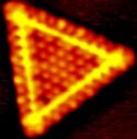
The first atomic-scale images of nanocrystals that help reduce pollution show a surprising triangular, rather than hexagonal, shape. The new information should help researchers improve the chemical process.
Click for larger version
Phys. Rev. Lett. 84, 951 (2000). Atomic-Scale Structure of Single-Layer MoS2 Nanoclusters. S. Helveg, J. V. Lauritsen, E. L�gsgaard, I. Stensgaard, J. K. N�rskov, B. S. Clausen, H. Tops�e, and F. Besenbacher
Thanks to Physical Review Letters & Dr. Flemming Besenbacher, University of Aarhus, Denmark © American Physical Society
|
Nanocrystals: Nanoscale crystals that are often harder, stronger and more wear resistant than the same materials in bulk form. "Nanocrystals might be used to make super-strong and long-lasting metal parts. The crystals also might be added to plastics and other metals to make new types of composite structures for everything from cars to electronics." See
Discovery could bring widespread uses for 'nanocrystals'. Single atoms caged inside nanocrystals gives you a "quantum confined atom", or QCA, "with potential uses ranging from clear-glass sunglasses to bio-sensors to optical computing and just about anything optical in between." See
Nanocrystals Technology Shines New Light on Optics, A Good Look at Nanocrystals, and Researchers Turn Scrap to Strength with Nanocrystals.
|
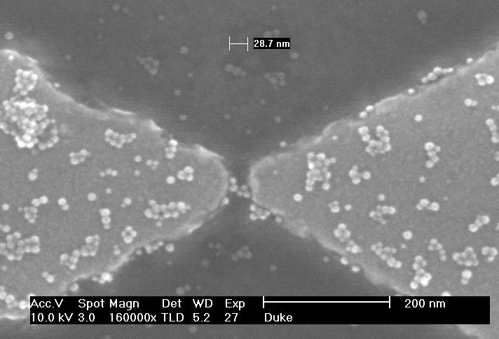
Single-electron transistor (SET) is a three terminal device, where single electron current between a source and a drain through a nanocrystal is controlled by a gate. The nanocrystals are the tiny light specs.
Click for larger version
Thanks to Professor Gleb Finkelstein, Physics Department. © Duke University
|
Nanoshells: Nanoscale metal spheres, which can absorb or scatter light at virtually any wavelength.
"The nanoshells act as an amazingly versatile optical component on the nanometer scale: they may provide a whole new approach to optical materials and components," Professor Naomi Halas. See Metal Nanoshells in Bioengineering and
Nanoshells May Be Key To Next Wave Of Light-Based Technology and
Physics of Nanoshells.
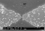
Nanohorns: One of the SWNT (single walled carbon nanotube) types, with an irregular horn-like shape, which may be a critical component of a new generation of fuel cells.
"The main characteristic of the carbon nanohorns is that when many of the nanohorns group together an aggregate (a secondary particle) of about 100 nanometers is created. The advantage being, that when used as an electrode for a fuel cell, not only is the surface area extremely large, but also, it is easy for the gas and liquid to permeate to the inside. In addition, compared with normal nanotubes, because the nanohorns are easily prepared with high purity it is expected to become a low-cost raw material." See
NEC uses Carbon Nanotubes to Develop a Tiny Fuel Cell for Mobile Applications and here is a
TEM image.
Nanowires: "Semiconductor nanowires are one-dimensional structures, with unique electrical and optical properties, that are used as building blocks in nanoscale devices." See
Nanowires within nanowires and
Learning how to Fabricate Nanowire.
"Striped or 'superlatticed' nanowires can function as transistors, LEDs (light-emitting diodes) and other optoelectronic devices, biochemical sensors, heat-pumping thermoelectric devices, or all of the above, along the same length of wire." See
Nanowires Get Their Stripes.
Nanosprings: A nanowire wrapped into a helix. Speculation is that they
"may someday make highly sensitive magnetic field detectors, perhaps finding application in hard drive read heads. Alternatively, nanosprings could serve as positioners, or even as tiny conventional springs, for nanomachines of the future." See
Spiraling in on Nanosprings
and
Nanosprings jump into place.
|
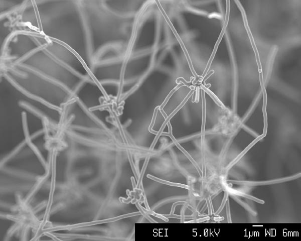
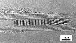
Vapour grown carbon fibres are obtained as shown in this SEM image. The diameters of these fibres can vary from 100 nm to 500 nm.

Click for larger version
Thanks to Charanjeet Singh, Polymer Research Group, Department of Materials Science & Metallurgy © Cambridge University
|
Nanomesh and Nanofibres: (or "Nanofibers") This term covers CNT's (see above), and as described here, the other "nanoscale fibers" referred to as "polymeric" (made from polymers). Currently used in air and liquid filtration applications. Using a process called "electrospinning" - or e-spin - a polymer "mesh" is formed into a nanofiber membrane, hense "nanomesh", with 150 - 200 nm diameters. Some have been made since 1970, but were not called "nano" until recently. One potential use is "to prevent body tissues from sticking together as they heal. It also breaks down in the body over time like biodegradable sutures." , which makes it a surgical material for the 21st Century. Other uses include biomedical devices, filtration systems, and dust collecting systems. See Biodegradable nanofiber could prevent scar tissue.
|
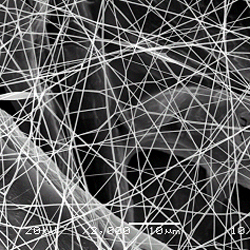
"Ultra-Web(R) nanofiber" produced on a Scanning Electron Microscope (SEM).

Click for larger version
Thanks to Nanofiber Media Products. © Donaldson Company, Inc.
|
Nanorods: Another nanoscale material with unique and promising physical properties, such that may yield improvements in high-density data storage, and allow for cheaper flexible solar cells. See
Three Element Nanorods and Flexible and Inexpensive Solar Cells Based on Inorganic Nanorods.
Nanopores: Essentially itty bitty tiny holes. Nanoscopic pores found in purpose-built filters, sensors, or diffraction gratings to make them function better. See
Influencing structure in the heart of nanoland. As activated carbon, they may also be used as an alternative fuel storage medium, due to their massive internal surface area.
"Scientists believe nanopores, tiny holes that allow DNA to pass through one strand at a time, will make DNA sequencing more efficient." See
Understanding Nanodevices -- Nanopores. In biology, they are
"complex protein assemblies that span cell membranes and allow ionic transport across the otherwise impermeable lipid bilayer. Nanopores are important because while some pores help maintain cell homeostasis, others disrupt cell function." See
Towards Fabrication of Solid-State Mimics of Biological Nanopores.
"A nanopore can be a protein channel in a lipid bilayer or an extremely small isolated 'hole' in a thin, solid-state membrane" such that "DNA and RNA, can be registered and characterized singly ..." See
Developing Nanopores as Probes and
The Nanopore Project.
|
Nano-test-tubes: CNT's opened and filled with materials, and used to carry out chemical reactions. See
The Opening and Filling of Multi-Walled Carbon Nanotubes (MWTs) and The Opening and Filling of Single-Walled Carbon Nanotubes (SWTs).
|
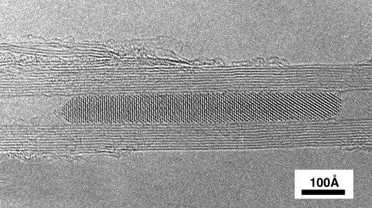
A High Resolution Transition Electron Micrograph (TEM) of Samarium Oxide Inside a Multi-Walled Carbon Nanotube.
Click for larger version
Thanks to Professor W. Graham Richards, Chairman of Chemistry. © University of Oxford
|
Nanofilters: One opportunity for nanoscale filters is for the separation of molecules, such as proteins or DNA, for research in genomics. See
Selective nanofilters for proteins, DNA Another, as
"masks to prevent exposure to biological pathogens such as viruses that can be as small as 30 nanometers in diameter." See
Biologically inspired nanotechnology. And another use is in water filtration. See Softer, Purer Water.
Nanopens & Nanopencils: (AKA: Atomic Pencil)
"Analogous to using a quill pen but on a billionth the scale", and may transform dip-pen nanolithography. Allows for drawing electronic circuits a thousand times smaller than current ones. The "pen" is an atomic force microscope (AFM). See Nanopipettes and Nanoplotter for further details.
Nanopipettes: "Cantilevered/Straight Nanopipettes can be used as nanopens for controlled chemical delivery or removal from regions as small as 100 nanometers. They can also be used as vessels for containing molecules whose optical properties change in response to their chemical environment." Other uses include
"controlled chemical etching with the precision of atomic force microscopy; chemical imaging of surfaces; delivering femtosecond laser pulses; and performing NSOM/SNOM imaging using a UV excimer laser." See
Cantilevered/Straight Nanopipettes Modifying the nanopipette yields other nanotools, such as Nanotweezers and Nanoheaters. See
Nanotools.
Nanoplotter: A multi-tip nanopen.
"A device that can draw patterns of tiny lines just 30 molecules thick and a single molecule high. ... produces eight identical patterns at once and extends ... dip-pen nanolithography towards mass producing nanoscale devices and circuits by converting what was a serial process to a parallel one. May be use to
"... miniaturize electronic circuits, pattern precise arrays of organic and biomolecules such as DNA and put thousands of different medical sensors on an area much tinier than the head of a pin." See
Plotting Chemicals and
Nanoplotter with Parallel Writing Capabilities (PDF).
|
Nanobalance: Simply put, a nanoscale balance for determining mass, small enough to weigh viruses and other sub-micron scale particles. "A mass attached at the end of a nanotube shifts its resonance frequency. If the nanotube is calibrated (i.e., its spring constant known), it is possible to measure the mass of the attached particle." A nanobalance "could be useful for determining the mass of other objects on the femtogram to picogram size range." See Weighing The Very Small.
|
Transmission electron microscope image shows "nanobalance:" a resonating carbon nanotube used to determine the mass of the attached carbon particle.
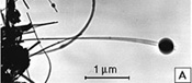
Click for larger version
Thanks to John Toon, Georgia Institute of Technology. © Science Magazine
|
Nanobeads: Polymer beads with diameters of between 0.1 to 10 micrometers. Also called nanodots, nanocrystals and quantum beads.
Impregnating fluorescent crystal chips into these beads allows simultaneous measurement of thousands of biological interactions, a stepping stone for breakthroughs in the diagnosis and treatment of disease. ... with the potential to accelerate drug discovery and clinical diagnostics." See
Nanodots and
Local Mechanical Properties of Cells.
|
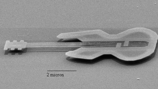
Nanoguitar: "Made for fun to illustrate the technology -- the world's smallest guitar is 10 micrometers long -- about the size of a single cell -- with six strings each about 50 nanometers, or 100 atoms, wide. Just one of several structures that Cornell researchers believe are the world's smallest silicon mechanical devices. Researchers made these devices at the Cornell Nanofabrication Facility, bringing microelectromechanical devices, or MEMS, to a new, even smaller scale -- the nano-sized world." See World's smallest silicon mechanical devices are made at Cornell.
|
Smallest guitar, about the size of a human blood cell, carved out of crystalline silicon, illustrates new technology for nanosized electromechanical devices.
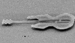
Click for larger version
Thanks to Professor Harold Craighead and Dustin Carr. © Cornell University
|