Home > Nanotechnology Columns > UAlbany College of Nanoscale Science and Engineering > Materials Characterization and Nanoscale Materials
 |
Alain Diebold Professor of Nanoscale Science UAlbany College of Nanoscale Science and Engineering |
Abstract:
Nanoscale materials have opened a rich new world of possibilities for science and engineering. In a discussion of nanoscale materials it is useful to divide them into ultra-thin films, ultra thin wires, and nano scale dots. These nano films, wires and dots all exhibit new phenomena which is the origin of the richness.
April 6th, 2010
Materials Characterization and Nanoscale Materials
Nanoscale materials have opened a rich new world of possibilities for science and engineering. In a discussion of nanoscale materials it is useful to divide them into ultra-thin films, ultra thin wires, and nano scale dots. These nano films, wires and dots all exhibit new phenomena which is the origin of the richness. Research, development, and manufacture of nanoscale materials all require advances in materials characterization including microscopy and physical/electrical characterization. In order to perform these measurements, one must both improve the measurement and understand how to interpret the impact of nanoscale phenomena on the measurement. The goal of this article is to provide a brief discussion of some of the key methods used to characterize nanoscale materials. All of these methods work together to provide a complete picture of nanoscale materials and their properties.
In addition to their size, nanoscale materials all have a more surface area than bulk samples. When nanoscale materials are assembled into a composite material, interfacial layers can change their properties. Today's nanoscale transistors provide a well known example of the impact of interfacial layers. In a transistor, the gate starts at the silicon wafer and includes the transistor channel, interfacial oxide, high k, and then the metal gate electrode (often called the gate stack). Reducing the transistor dimensions required replacing silicon dioxide (actually silicon oxynitride) with a high k film. Experience has shown that an interfacial oxide layer was required before depositing the high k film. Because the interfacial oxide is only a few monolayers thick, characterizing it is very challenging. It is important to note that despite the nanoscale size of this layer, it has a very big impact on the electrical properties of the transistor. Thus characterizing and controlling it is critical.
Several key materials characterization methods and their relationship to nanoscale thin films are discussed below. The College of Nanoscale Science and Engineering (CNSE) routinely uses these methods in academic research and for the R&D it does with its partners such as IBM, TEL, Applied Materials, and ASML.
Nanoscale Metrology for Nanoscale Films
As mentioned above, nanoscale films are often one film in a stack of thin film layers. Often, some of the films are opaque or the films stack complicated enough to require characterizing these films through a variety of methods. Below, we discuss optical, X-Ray, and Ion Beam methods that one typically uses to characterize the transistor gate stack.
Optical Measurements
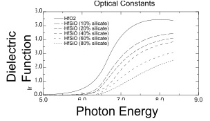
A variety of optical measurements are useful for nanoscale films. Ellipsometry, photoreflectance, and second harmonic generation have all been used to characterize nanoscale materials. Ellipsometry is frequently used to measure the thickness of dielectric, semiconductor and thin metal films. It can also determine the dielectric function of new materials when the thickness is known. The dielectric function of the high k films changes with the composition of the film. For example, the amount to silicate in hafnium silicate and the process conditions both have a strong impact on the dielectric function and thus optical response as shown in figure 1. Ellipsometry is an excellent means of controlling manufacturing processes such as those used to fabricate the gate stack. Photoreflectance provides a means of characterizing the stress in single crystal semiconductor films. This method is well suited to characterizing silicon-germanium films used as the transistor channel. Second harmonic generation is a useful method of characterizing interfacial properties especially ones between a dielectric and semiconductor.
 |
X-Ray Measurements
X-Ray reflectivity (XRR), X-Ray Diffraction (XRD), X-Ray Fluorescence (XRF) and X-Ray Photoelectron Spectroscopy (XPS) all provide important means of characterizing nanoscale materials. XRR measures film thickness and works well with metal films which are opaque to ellipsometry. XRR is often applied to transistor gate stack measurements and is especially helpful when the top layer in a stack is a metal film. XRD and high resolution XRD provide information about the crystal structure of thick and thin films and grazing incidence XRD can tell us if nanoscale films have begun to crystalize. After deposition, the high k film is typically amorphous. HR-XRD is essential when doing research and development of new materials such as silicon-germanium thin films. XRF measures the amount of an element present in films is frequently used during semiconductor manufacturing to control the composition of thin films. X-Ray Photoelectron Spectroscopy (XPS) has proved essential for understanding the chemical state of high k film stacks. Depth profiles determined using angle dependent XPS provide a picture of the inter-diffusion of film stack components. An XPS depth profiles is shown in Figure 1. Often the high k films contain nitrogen, and XPS is an excellent means of determining the nitrogen concentration.
Ion Beam Methods
Rutherford backscattering and other high energy ion beam methods measure key parameters of the gate film stack. Recently, CNSE added High Resolution Rutherford Backscattering which provides much better depth resolution. This method will greatly enhance CNSE's RBS capability. Another ion beam method, secondary ion mass spectrometry, proves both depth profiles and trace contamination analysis.
Multiple Methods = Better Film Characterization
Through use of multiple methods, CNSE is able to provide thorough characterization of film stacks and remove any ambiguities that one may find by using a single method. In the transition from Lab to Fab, the thorough film characterization applied during research is put into practice inside CNSE's cleanroom to further the R&D efforts of CNSE's partners. Research partnerships such as the one my group has with TEL offer a great opportunity for graduate students to see first hand how industry research and development is done. CNSE partners gain through direct access to leading edge research.
Bookmark:


|
|
||
|
|
||
| The latest news from around the world, FREE | ||
|
|
||
|
|
||
| Premium Products | ||
|
|
||
|
Only the news you want to read!
Learn More |
||
|
|
||
|
Full-service, expert consulting
Learn More |
||
|
|
||