Home > Nanotechnology Columns > UAlbany College of Nanoscale Science and Engineering > Post-CMOS Nanoelectronics: Primetime for nanotechnology solutions
 |
Robert Geer CNSE Vice President for Academic Affairs and CNSE Chief Academic Officer; Professor of Nanoscale Science University at Albany-College of Nanoscale Science and Engineering |
Abstract:
Computer chips are what make �smart technology' smart. And silicon-based CMOS nanoelectronics comprise the neurons of those electronic brains. Arguably the world's most transformative technology in terms of economic, cultural and social impact, silicon CMOS continues to plunge to ever-smaller device dimensions and ever-expanding levels of integration. And although technologists have long predicted the end of the technological �run' of CMOS advancement - often referred to as Moore's Law - the fundamental physics of energy dissipation in nanoscale Si transistors and Cu wiring on today's most advanced chips may well be a challenge that cannot be answered by Si nanoelectronics.
February 4th, 2010
Post-CMOS Nanoelectronics: Primetime for nanotechnology solutions
Computer chips are what make �smart technology' smart. And silicon-based CMOS nanoelectronics comprise the neurons of those electronic brains. Arguably the world's most transformative technology in terms of economic, cultural and social impact, silicon CMOS continues to plunge to ever-smaller device dimensions and ever-expanding levels of integration. And although technologists have long predicted the end of the technological �run' of CMOS advancement - often referred to as Moore's Law - the fundamental physics of energy dissipation in nanoscale Si transistors and Cu wiring on today's most advanced chips may well be a challenge that cannot be answered by Si nanoelectronics. Indeed, it is not likely that any conventional charge-based switch - no matter what the material - will dramatically alter the cost per function curve that drives today's integrated circuit (IC) technology, since resistive and capacitive parasitics intrinsic to IC topologies effectively dominate system performance.
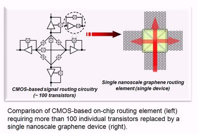
To put it bluntly, it looks as if a new nanoelectronic switch will be needed. Considering the tremendous cost required to retool an entire industry for such a fundamental technology change, a new switch cannot simply be 30% or 50% faster than - or consume half the power of - a Si FET. Its system performance and extendibility must be measured in orders of magnitude. It is hardly a surprise, then, that nanotechnology is providing some of the most provocative solutions to address this challenge. The core of these solutions - being pursued by many of the world's leading university/industry/government research consortia, such as CNSE's Institute for Nanoelectronics Discovery and Exploration (INDEX) - is to exploit nanotechnology to replace multiple CMOS switches with a single nanoscale logic element, i.e. a multi-function nanoscale gate. Perhaps the best example is the use of a single atomic monolayer of carbon - graphene - not as a semiconductor, but as an electron waveguide which can focus and direct electrons much like photons are directed in optical fibers and lenses. The so-called Veselago lens effect (described in 2007 by Cheianov and coworkers) in graphene has the potential to combine devices and interconnects in the same atomic monolayer constituting an ultra-low power field-programmable gate array (FPGA). In this scenario, a single graphene focusing switch + interconnect could replace as many as 200 conventional transistors. Researchers at CNSE's INDEX Center are at the forefront of this critical development.
A similar nanotechnology-enabled solution to the challenge facing conventional Si CMOS technology may come not from manipulating the electron via its charge, but via its intrinsic magnetic properties (so-called �spin'). Spin is an intrinsically quantum mechanical property. The nanotechnology of spin and magnetism is what allows us to store more than one trillion bits of information on hard drives no larger than a person's wallet. And now, that same nanotechnology may be able to enable the logic operations that process those 1 trillion bits as well. A dynamically reprogrammable logic gate (proposed by Sham and coworkers in 2007) relies solely on spin-based information transmission (not electric charge). In principle, this type of gate can be employed in a cascading architecture and support the same design fabrics that have been developed for Si CMOS over the last 20 years while, perhaps, avoiding challenges associated with conventional CMOS power dissipation. The fundamental nanoscale science and engineering breakthroughs necessary to explore this potential are also a focus of CNSE's INDEX initiative, along with similar research consortia across the globe.
 |
So, while Si CMOS-based nanoelectronics is facing its share of technology challenges, the ever-expanding knowledge base of nanotechnology has no shortage of game-changing alternatives from which to respond. Should you trade in your Si chip for one made of carbon or one processing electron spin instead of electron charge? Not yet. No technology known to mankind has been as successful as Si nanoelectronics and it will be around for a long while. But don't be surprised if R&D on carbon or spin-based devices starts to become more �D' than �R'.
Bookmark:


|
|
||
|
|
||
| The latest news from around the world, FREE | ||
|
|
||
|
|
||
| Premium Products | ||
|
|
||
|
Only the news you want to read!
Learn More |
||
|
|
||
|
Full-service, expert consulting
Learn More |
||
|
|
||