Home > Nanotechnology Columns > Kos Galatsis > The Eyes and Ears of Nanotechnology
 |
Kos Galatsis Chief Operating Officer FENA and WIN Centers, UCLA |
Abstract:
In the push for ubiquitous nanotechnology in the 21st century, may of us take for granted the science and technology that takes place behind the scenes. To make useful nanoproducts, one generally requires a) advanced nanomaterials, b) sophisticated fabrication tools and processes and c) integrated metrology tools and modeling. Let's look at the eyes and ears of nanotechnology, that being "metrology".
January 20th, 2009
The Eyes and Ears of Nanotechnology
In the push for ubiquitous nanotechnology in the 21st century, may of us take for granted the science and technology that takes place behind the scenes. To make useful nanoproducts, one generally requires a) advanced nanomaterials, b) sophisticated fabrication tools and processes and c) integrated metrology tools and modeling. Let's look at the eyes and ears of nanotechnology, that being "metrology". Metrology in nanotechnology refers to the measurement at nanometer length scales. Doing so isn't trivial and some challenges that need to dealt with includes: 1) devising ways of managing new nanomaterial platforms (for instance, such as graphene) 2) measuring defects of nanomaterials 3) measuring critical dimensions and material thickness 4) measuring interfacial nanomaterial properties 5) measuring high aspect ratio nanostructures, and 6) calibrating metrology tools to certain test nanostructures. Some impressive capabilities exist that allows one to measure various materials properties. However, as the nanomaterial space continues to expand (graphene, strongly correlated materials, ferromagnetic materials, biomaterials, hybrid structures, etc�), tools are continuously being challenged.
Over a decade ago, the atomic force microscope (AFM) emerged as a leading method to probe topology of structures at nanoscale dimensions. Since then, scanning probe microscopy has become not only a topographic imaging tool with sub-Angstrom resolution, but its abilities have been extended to include measuring intrinsic mechanical and electrical properties of materials. But even still today, the resistance map obtained by an AFM still makes it difficult to characterize typical semiconductor parameters of interest such as doping profile or types of dopants (p or n). Other capabilities have emerged like the special way (near field �tunneling') in which a scanned probe couples to electromagnetic radiation can be used to extract local information about plasmons for emerging plasmonic devices. Another important area for materials is the quantitative measure of elasticity. This is performed by a nano-indenter, a tool which presses into a surface while accurately measuring the depth into the surface and the downward applied force. Although known as a nanoindentor, the tool typically has only micron spatial resolution. Veeco, working in conjunction with Dow Chemical, has now pioneered a true �nano' indenter by using an AFM with a special cantilever and a calibrated tip size and geometry. Using similar theory of the nanoindentor applied to an AFM, they are able to quantify the elastic modulus of a variety materials including polymers, carbon films, and semiconductor samples at much smaller length scales than previously possible (see Fig. 1).
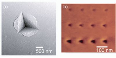 |
| (a) AFM image of a indentation (b) Specific cantilever indents a thin carbon film |
Instead of indenting a surface, one can also study mechanical properties by driving the AFM tip so that it taps on the surface. Normally in this �tapping' mode, one measures average impulse. Higher harmonics of the drive frequency are generated during the repulsive impulse which can uniquely determine the �hardness' or elasticity of a surface at the nanoscale. It should be mentioned that force microscopy has evolved to include Piezoresponse Force Microscopy (PFM), Electric Field Microscopy (EFM), Variable Temperature Magnetic Field Microscopy (VT-MFM) and others.
Mature technologies such as x-ray, neutron, and electron scattering have made consistent advances to keep pace with metrology challenges brought to the community by new nanotechnology research. Unlike visible light, x-rays have the disadvantage of very small elastic scattering cross-section in materials (index of refraction nearly 1 for most materials), thus making refractive optics difficult. Diffractive optics are becoming a popular alternative, with spatial resolution now reaching below 30nm.
However, limited scattering of x-rays allows the study of both buried interfaces and intrinsic material composition. Measuring the diffraction off the lattice or other periodic structures (such as lithographic features) the details of shape and even distortions in the lattice (strain fields) can be observed. Although x-rays only weakly scatter, heavier materials scatter more photons than lighter materials so image contrast can be achieved. In Fig. 2, 3-d images are shown of IC copper interconnects and strain fields in metal particles reconstructed from various algorithms.
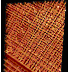 |
| Image of metal interconnects of a microprocessor - x-ray scattering from metal and dielectric. |
Additionally, material composition can also be determined through inelastic scattering of the x-rays on the inner shell electrons (x-ray fluorescence provides fingerprint for atoms and molecules). Reflected x-rays at glancing incidence can provide a measure of critical dimensions and roughness of small that make up the building block of nanoelectronics. This provides an encouraging route forward to beyond CMOS where more complex 3D structures are envisioned and where tolerances would be a greater concern.
Although electrons and x-rays employ the same elastic and inelastic scattering principles to measure material properties, they have very different interaction cross sections which provides advantages for each. Due to the ease of focusing electrons compared with x-rays, the spatial resolution of a STEM is currently unrivaled by x-rays. However, for larger sample volumes (micron or larger samples) which require less resolution (~30nm), x-rays may provide significant advantages in terms of speed and volume of data collection. Similarly, because of the lack of interaction of the x-ray, they are commonly thought as less damaging than electron beams. However, if one normalizes the damage events by the number of useful (elastic) imaging events, electron beams actually tend to damage materials less.
As expected for two rival techniques, both are being widely used for nanotechnology metrology. With x-rays, the key technical challenges include focusing the x-rays to a smaller beam for finer resolution. Also, there is significant work to be done to understand coherent scattering from x-rays and dynamic evolution for time dependent studies of nanostructures. For electron beams, pushing the forefront in atomic scale tomography and angstrom level resolution are some of the goals for the next generation STEM. Amazingly, to get to atomic scale tomography one must be able to tilt the sample with angstrom level precision, posing a significant challenge. Also, further correcting the lens aberration of the electron beam should allow more resolution and contrast to the images.
Bookmark:


|
|
||
|
|
||
| The latest news from around the world, FREE | ||
|
|
||
|
|
||
| Premium Products | ||
|
|
||
|
Only the news you want to read!
Learn More |
||
|
|
||
|
Full-service, expert consulting
Learn More |
||
|
|
||