Home > Nanotechnology Columns > Kos Galatsis > Nanopatterning - saving Moore's Law
 |
Kos Galatsis Chief Operating Officer FENA and WIN Centers, UCLA |
Abstract:
A major contributor to the semiconductor industry's success in sustaining Moore's Law is attributed to the advancement of lithography technology. Lithography is used to create features and patterns for devices, vias and interconnects that contribute to a working microprocessor, memory or application specific integrated circuits. The semiconductor industry is often referred to as the backbone of the information age, generating worldwide revenues of $256B in 2007. Lithography is the single largest cost factor in the manufacturing food chain, and hence being the most important.
October 16th, 2008
Nanopatterning - saving Moore's Law
A major contributor to the semiconductor industry's success in sustaining Moore's Law is attributed to the advancement of lithography technology. Lithography is used to create features and patterns for devices, vias and interconnects that contribute to a working microprocessor, memory or application specific integrated circuits. The semiconductor industry is often referred to as the backbone of the information age, generating worldwide revenues of $256B in 2007. Lithography is the single largest cost factor in the manufacturing food chain, and hence being the most important. Current state of the art patterning is based on lithography technology capable of creating 45 nm feature sizes. Production of the 45 nm-node technology was introduced in 2007 pioneered by IBM and Intel. This platform is based on 193nm wavelength light that is capable of producing features down to 45nm. Semiconductor fabs are incorporating immersion technology to achieve pattern dimensions well below the resolution of the wavelength used to create the feature sizes (going beyond the traditional Rayleigh limit), in which the air gap between the light source and the mask is filled with a higher index liquid, allowing for smaller feature sizes to be achieved. Next generation lithography systems are planned to be based on extreme ultraviolet (EUV) which promises to give the industry the quantum leap forward into the 22nm node. EUV will incorporate a much smaller operating wavelength of only 13.5nm (see Figure 1).
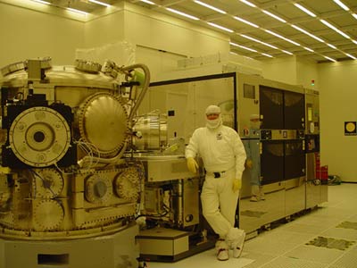 |
| EUV prototype system developed by Intel. |
Working with such a shorter wavelength has resulted in hampered development of adequate light sources, resists and mask blanks. From an economic point of view, profound changes are also expected with the change to EUV, for instance, tools are expected to fetch up to $100M as opposed to current 193nm immersion tools that sell for a mere $30M.
Not only is creating nano-dimensional feature sizes challenging, but device yield and performance become increasingly sensitive to smaller amounts of process and dimensional variations. Therefore, as conventional CMOS scaling approaches the atomic and molecular levels, questions such as "Can self-assembly based technologies offer advantages beyond conventional top-down lithography approaches?" and "Do alternative patterning techniques favorably couple to alternative nanoarchitectures for beyond CMOS information processing?" warrant discussion.
One exciting approach forward is by creating nanopatterns and templates via self-assembly methods. Self-assembly methods can be divided up into two distinct functional cases. (1) sacrificial processes, where the nanocomponents responsible for self-assembly are sacrificed (destroyed) and do not actively participate in the function of the nanostructure (such as self-assembled templates) and (2) active processes, where the nanocomponents responsible for self-assembly are also used as active elements within an integrated circuit and remain there for the life of the structure. An example is PNA conjugation, where the PNA is responsible in conjugating with another PNA in creating useful 2 and 3 terminal devices. (see Figure 2).
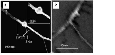 |
| Two and three terminal structures made by conjugating CNT with PNA. M.Ozkan (UCR) |
Di-block copolymer technology is an example of a sacrificial self-assembly process, and thus used as a template. The copolymers are two different types of polymer chains connected at one end with a covalent bond such as polystyrene and poly(methyl methacrylate) (otherwise known as PMMA). The two polymers that constitute the material spontaneously form ordered structures with domain dimensions of 5-50nm. The size and shape of the domains are dependent on the molecular weight and composition of the copolymer and typically assume morphologies of lamellae, spheres and cylinders.
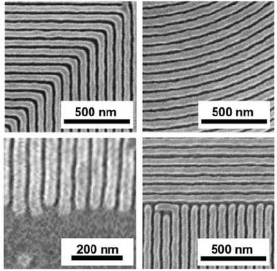 |
| Various di-block copolymer shapes for nanopatterning. P.Nealey (Wisconsin) |
Viruses have also been used for creating useful nanopatterns. Viruses are part of the biological family and have been used for highly specific molecular recognition capabilities that can be programmed through genetic engineering. A popular biomaterial used for this purpose has been the M13 bacteriophage. A bacteriophage is a bacterial virus made up of a single-stranded DNA enclosed with a protein hull. The length of the virus can be up to 1 um and has a diameter of about 10nm. The virus can be bio-engineered to selectively self-assembly with specific nanoparticle metals and quantum dots.(see Figure 4)
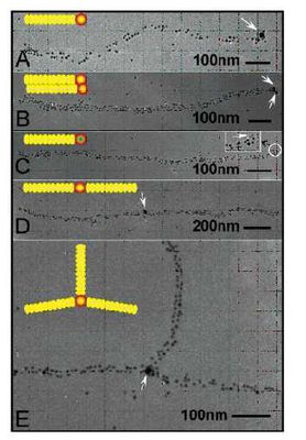 |
| Images of bacteriophage with Au and CdSe particles assembled in various ways. Huang (UCLA) |
A key area where alternative patterning techniques could benefit and offer an advanatge over conventional top-down lithography is in the space of alternative nanoarchitectures for beyond CMOS information processing. Such architectures include neural networks (bi-inspired architectures) and self-healing fault tolerant approaches. For instance, CNT crossbar assembly via nanosphere dot lithography has been shown useful in photonic crystals, DNA self-assembled has been shown conducive for active network based architectures which are able to overcome imperfect assembly and defects of DNA and the assembly of crossbar architectures hold promise to have superior density properties when fabricated using self-assembled CNTs and nanowires. Some examples of alternative architectures are presented in Figure 5 together with possible alternative patterning techniques that would be conducive in realizing these architectures.
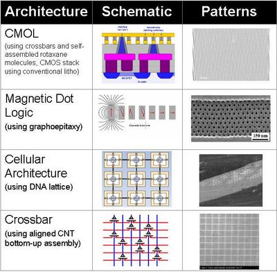 |
| Various architectures derived by alternative patterning methods. |
Although conventional top-down lithography has dominated patterning 2D planar structures for integrated circuits over the past 50 years, alternative patterning techniques such as those driven by self-assembly processes will only become ubiquitous if driven by nanoarchitecture requirements. There are few proof-of-concept nanoarchitecture examples that have been demonstrated that would make the semiconductor industry take notice and seriously commit to more exotic alternative patterning technology development to ensure Moore's law survives down to molecular and atomic scales.
Bookmark:


|
|
||
|
|
||
| The latest news from around the world, FREE | ||
|
|
||
|
|
||
| Premium Products | ||
|
|
||
|
Only the news you want to read!
Learn More |
||
|
|
||
|
Full-service, expert consulting
Learn More |
||
|
|
||