Home > Nanotechnology Columns > UAlbany College of Nanoscale Science and Engineering > Advancing Nanoscience through R&D Consortia
 |
Chris Borst Process Engineering Manager UAlbany- College of Nanoscale Science & Engineering |
Abstract:
Although the terms �nanoscale' and �nanoscience' have recently found common use, the semiconductor industry has been finding solutions to roadblocks and challenges on the nanometer level for the past several decades. The fundamental building block of the semiconductor devices used in computers, cell phones, and other high tech devices, is the complimentary metal-oxide semiconductor (CMOS) transistor.
March 25th, 2008
Advancing Nanoscience through R&D Consortia
Although the terms �nanoscale' and �nanoscience' have recently found common use, the semiconductor industry has been finding solutions to roadblocks and challenges on the nanometer level for the past several decades. The fundamental building block of the semiconductor devices used in computers, cell phones, and other high tech devices, is the complimentary metal-oxide semiconductor (CMOS) transistor. The CMOS transistors in high technology on the market today require a gate oxide dielectric thickness of less than 2 nanometers (nm), or ~5 atoms, of physical thickness.
As gate thickness shrinks, the overall size or width of devices follows suit, resulting in a smaller transistor area, and exponentially increasing the number of transistors that can be placed on a chip to power a laptop or support handheld internet browsing on a cell phone. This is the basis of Moore's Law, and has a cascading impact on the development of other processes used to support and connect CMOS transistors. Reducing gate thickness is but one of hundreds of processes that now require research, understanding, and development at physical dimensions (width, depth, length) of tens of nanometers. Keeping up with the predictions of Moore's Law is becoming more costly each year. Figure 1 shows the rising cost of semiconductor research and development (R&D) since 1990. Total R&D costs were $45 billion in 2006, and are predicted to reach $100 billion in 2010.
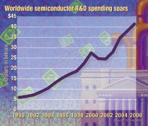 |
Figure 1 - Rising cost of worldwide semiconductor R&D. From M. LaPedus, "Schemes strip cost out of chip R&D", EE Times, July 16, 2007.
This rising cost has caused changes in many companies' approach to funding semiconductor R&D. While the largest and most cash-rich such as Intel and Samsung are still able to drive the effort internally, several companies have begun to either outsource R&D to overseas foundries or consolidate resources through consortia. A recent example of foundry outsourcing is seen in Texas Instruments' recent announcement to pursue future development nodes (45nm and beyond) at Taiwan Semiconductor Manufacturing Company (TSMC) and other foundry partners. This results in the elimination of jobs and a loss of internally-developed intellectual property (IP) which has become an important aspect of advanced semiconductor R&D. The second option, the research and development consortium, is seen by others as a more attractive option which allows the sharing of cash resources, expensive equipment, and intellectual property. A consortium allows several major companies that are not direct competitors to keep advancing development along the path of Moore's Law without shouldering the complete financial burden. At the forefront of the consortia concept is the Center for Semiconductor Research (CSR) at the University at Albany - SUNY College of Nanoscale Science and Engineering.
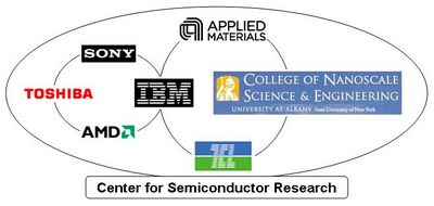 |
Figure 2 - Schematic diagram showing company / academic interaction through the U Albany CNSE Center for Semiconductor Research.
The CSR was established in May 2005 as a partnership between industry-leading chip makers, tool suppliers, and university researchers. It is a long-term joint R&D cooperative program on future computer chip technology nodes. The CSR is the only center within a university setting that provides the full vertical integration of design, modeling, fabrication, testing, and pilot-prototyping capabilities required to produce functional demonstrations of semiconductor devices at the most aggressive technology nodes. Industry partners within the CSR include IBM, Advanced Micro Devices, SONY, Toshiba, Tokyo Electron, and Applied Materials.
The success of the CSR consortium depends on its ability to bring timely solutions to advanced semiconductor R&D challenges to market. The integrated-circuit manufacturers need to develop the processes and IP required to surmount the nano-scale device challenges described previously, and the tool suppliers need to develop, test, and prove their tools as a vital part of a successful manufacturing process flow. The measure of success in the semiconductor industry has always been results - papers published, patents filed, and prototypes created. The measure of success for the academic partners is equally results-oriented. As the industry partners prove technology for current-node manufacturing, the university partners are able to delve into the fundamental aspects of the science involved at the nanoscale, and apply learning and advanced processing techniques to other areas of nanoscience such as nanobiology and spintronics. Some results of nano-scale processing successes achieved within the CSR consortium are illustrated below.
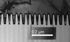 |
Figure 3 - Pattern, etch, and metal fill of trenches with a single-trench width of approximately 22 nanometers. From C. Borst, et. al, "Driving Metallization Dimensions to Sub-30nm using Immersion Lithography and a Self-Aligned Double Patterning Scheme", 24th Advanced Metallization Conference, October 9, 2007.
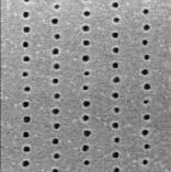 |
Figure 4 - Pattern and etch, of circular via/contact holes with a width of approximately 20 nanometers. From J. Miao et. al, "Double Patterning Combined with Shrink Technique to Extend ArF Lithography for Contact Holes to 22nm Node and Beyond", SPIE Advanced Lithography, February 2008.
The path of interconnection of the billions of CMOS transistors at the silicon level to the device package / circuit board in your computer or cell phone is through millions of nanoscale metal wires. The building blocks of these wires are horizontal rectangular lines or �trenches' and circular vertical holes or �vias' filled with copper, aluminum, or tungsten metal. As the CMOS transistor gate thickness, width, and area decrease, the wires used to connect them must also decrease in size, creating a substantial challenge in lithographic printing, etch, and fill with metal.
Cooperative work at the CSR has generated the results in Figures 3 and 4, using the advanced processes and equipment available through the consortium. Figure 3 shows repeating 22nm wide trenches filled with copper. In order to electroplate the copper into such a small feature, an advanced atomic-layer deposition technique was used to first coat each trench bottom and sides with a metal layer on the order of 10 nanometers thick. The image in Figure 4 is of an array of circular vias printed using an advanced double-pass patterning technique combined with a circular via hole shrink process. The slight left/right offset between holes is due to the challenges of alignment between patterning passes. Double- patterning is presently at the forefront of R&D development for most process and equipment companies, and is a major focus being addressed within the CSR.
The trench and via structures demonstrated at ~22nm will find widespread use in high tech devices in approximately 5 to 10 years. This type of forward-directed work is what industry/academia development consortia hope to achieve, while sharing technology, IP, and incurred costs. Successes such as those described above support the concept that consortia-based research and development creates a viable path for nanoscience technology advancements in the years to come.
Bookmark:


|
|
||
|
|
||
| The latest news from around the world, FREE | ||
|
|
||
|
|
||
| Premium Products | ||
|
|
||
|
Only the news you want to read!
Learn More |
||
|
|
||
|
Full-service, expert consulting
Learn More |
||
|
|
||