Home > Nanotechnology Columns > Kos Galatsis > Appreciating the "nano" in chip manufacturing
 |
Kos Galatsis Chief Operating Officer FENA and WIN Centers, UCLA |
Abstract:
If its one industry that is steaming forward in nanotechnology, look no further than the semiconductor industry. The fact remains that this industry is by far the most sophisticated industry at the cutting edge of nanotechnology. With billions of dollars poured to built 60nm, 45nm and 32nm fabrication facilities, the semiconductor industry takes the prize in leading the "nano" way forward.
August 22nd, 2007
Appreciating the "nano" in chip manufacturing
If its one industry that is steaming forward in nanotechnology, look no further than the semiconductor industry. The fact remains that this industry is by far the most sophisticated industry at the cutting edge of nanotechnology. With billions of dollars poured to built 60nm, 45nm and 32nm fabrication facilities, the semiconductor industry takes the prize in leading the "nano" way forward.
Back in the 90's the semiconductor industry dominated microelectronics, crushing the 100 nm barrier sometime in 2004 when fabs kicked into the 90nm technology node. Mainstream computers today have chips with over 1 billion transistors and physical features with less than 90nm along with atomic accuracy and precision. To appreciate this further lets take a sneak preview of where some of the "nano"-magic lies in chip manufacturing.
One area where the nano-magic lies is in the patterning of nanostructures using lithography. Patterning and lithography is the bread and butter of semiconductor manufacturing. Most of the nano-magic happens in the litho tool. These tools are made up of complex cleaning, deposition and exposure stages that house precision optics to transfer nanopatterns from expensive masks (costing several millions $) to silicon wafers with diameters of 300mm. Typical throughput is a pumping 130 wafers per hour. Current lithography technology is dependant on 193nm wavelength light sources that are capable of producing features down to 65nm. By incorporating immersion technology, resolution below 40nm with accuracy at about 6nm is possible via tools made by ASML and Nikon. Next generation lithography systems are planned to be based on extreme ultraviolet (EUV) which promises to give the industry the quantum leap forward beyond the 22nm node. EUV will operate on a much shorter wavelength, 13.5nm compared to 193nm. Another difference is price, EUV tools are expected to fetch up to $100M as opposed to current 193nm tools that sell for a mere $30M. The cost and challenge is associated with the special light sources, photoresists and optics that are required to be developed to deal with the shorter 13.5nm wavelength, in addition to the precision mechanical controls required for nm alignment. Figure 1 gives you an idea of the shear size and complexity of a EUV lithography tool currently in development.
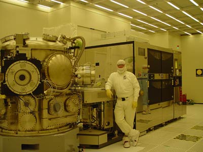 |
| EUV prototype system developed by Intel. |
To get a sense of the patterns produced by such a tool, Figure 2(a) shows an example of simple line structures that could possibly be used to make a wire to interconnect two devices or could be used to make up a device. At first glance the line seems straight and perfect, however with closer inspection, Figure 2(b) and 2(c), one can see rough line edges are imperfect sidewalls. The width of these lines are about 30nm with an average line width roughness of 5nm. The challenge is in creating lines with super smooth walls, razor sharp edges and structures that are flawless. As features shrink towards sub-nm these tasks become ever so more difficult.
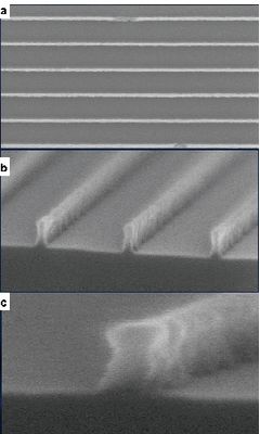 |
| Line patterns developed using photolithography. |
In order to produce a smaller transistor it is not sufficient to just shrink the transistors physical length and width, other dimensions must be shrunk as well. Shrinking gate lengths Lg, require thinner sidewall spacers Xs, shallower junctions Xje and Xjc, and most importantly thinner gate oxides Xg as shown in Figure 3(a). The gate stack is an important part of the transistor as it controls the field effect imposed on the transistor channel which is critical for desirable switching characteristics. Traditionally, the gate oxide material has been silicon dioxide which has scaled about 45 times smaller than the gate length. Figure 3(b) shows a real micrograph of a transistor with a gate length of 35nm. Figure 3(c) shows a micrograph of the critical dimensions of the gate stack where the oxide is only 1.2nm thick. These dimensions are so small that the atoms within the crystal lattice are visible.
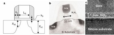 |
| Transistor challenges such as gate length and oxide thickness control are paramount. |
Advanced thermal oxidation and deposition technologies allows the fabrication of extremely thin oxide layers to be created with atomic layer of precision. As you would guess, since we are dealing with atomic thickness, one extra or less atomic layer will drastically effect the devices electrical properties, and hence that is exactly where the challenges and uncertainty lies with the industry, and by no means do solutions prop up as easy as a walk in the park.
Next time you power up your PC, don't forget to consider the elaborate nanotechnology that is behind your computing power which is ever so more taken for granted.
Bookmark:


|
|
||
|
|
||
| The latest news from around the world, FREE | ||
|
|
||
|
|
||
| Premium Products | ||
|
|
||
|
Only the news you want to read!
Learn More |
||
|
|
||
|
Full-service, expert consulting
Learn More |
||
|
|
||