Home > Nanotechnology Columns > UAlbany College of Nanoscale Science and Engineering > Determining Atomic Surface Structure Using Atomic Scale Imaging and First Principles Theory
 |
Vince LaBella Assistant Professor of Nanoscience College of Nanoscale Science & Engineering |
Abstract:
The atomic structure of surfaces and interfaces is becoming increasingly important for nanotechnology as physical dimensions of device structures are ultimately being pushed to the atomic limit. The scanning tunneling microscope (STM) has given profound insight into the nature of surfaces on the nano and atomic scale. However, interpreting STM images can be difficult due to several contrast mechanisms such as sample-tip convolution effects or bias-dependent variations in the local density of states (LDOS). However, when atomic scale STM images are combined with theoretically generated images from first principles calculations insight into the atomic arrangements can be made.
June 15th, 2007
Determining Atomic Surface Structure Using Atomic Scale Imaging and First Principles Theory
The atomic structure of surfaces and interfaces is becoming increasingly important for nanotechnology as physical dimensions of device structures are ultimately being pushed to the atomic limit. The scanning tunneling microscope (STM) has given profound insight into the nature of surfaces and interfaces on the nano and atomic scale. However, interpreting STM images can be difficult due to several contrast mechanisms such as sample-tip convolution effects or bias-dependent variations in the local density of states (LDOS). These mechanisms can confound the interpretation of image features, especially the determination of the atomic structure. However, when atomic scale STM images are combined with theoretically generated images from first principles calculations insight into the atomic structure can be made.
The STM can resolve atomic scale corrugations of a surface. It was invented in the early 1980's by Gerd Binnig and Heinrich Rohrer et al. at IBM's Zurich Research Laboratory. For this, Binnig and Rohrer were awarded the Nobel Prize for Physics in 1986. The operation of an STM is straightforward. Take a sharp metal tip and position it within a nanometer of a atomically clean conducting surface and apply a voltage bias across the tip and sample. Typically, the tip is atomically sharp but can also have a radius of curvature of a few nanometers. The electrons on the higher potential side will quantum mechanically tunnel through the vacuum barrier created by the tip-to-sample junction. This tunneling current is exponentially sensitive to both the tip-to-sample separation distance as well as the tip-to-sample voltage bias. It is this exponential dependence that gives STM its high degree of sensitivity and resolution. Small changes in height, or conductivity of the surface are reflected as large changes in the tunneling current.
To generate an image, the STM tip is moved or rastered across the surface while employing a closed loop feedback system to maintain a constant tunneling current by adjusting the height of the tip. If the current increases then the surface is closer and the tip is retracted, if it decreases then the surface is further away and the tip is extended. An image is a measure of the tip height values while the tip is rastered in both x and y. If the tip is sharp enough and the sample surface is clean, corrugations on the surface with sub nanometer or atomic resolution can be observed as shown in Fig. 1 and Fig. 2. The image generated is a map of constant tunneling probability or a surface of constant local charge density of the electrons. This makes determining the atomic positions from just an image difficult since corrugations in the charge density may or may not correspond to locations of the nuclei of the atoms.
To compare to the experimentally acquired images to help determine the atomic structure, first principles density functional theory (DFT) calculations are performed on a candidate atomic structure. However, DFT does not explicitly generate STM images. DFT solves the Kohn-Sham equations (which are of similar mathematical structure as the Schr�dinger equation) for a periodic arrangement of atoms. The calculations output both the equilibrium location of the nuclear cores (thus refining the guessed candidate structure) and the wave functions of all the electrons in space and energy. To generate a STM image, the probability density of the electrons (square modulus of the wavefunctions) must be integrated over the appropriate energetic limits. Pauli's exclusion principle states that only one electron with a given spin can occupy a state. Therefore, flow of an electronic current can only proceed via transitions of the electrons from occupied states in the STM tip into unoccupied states in the surface, or vice versa. Therefore the current at each position x and y is proportional to the wave functions integrated over an energy window that simulates the tip bias in the STM. Lastly, the height or z is obtained from a search procedure starting from infinity until the partial density equals some constant J whose value reflects the stationary STM current. This value of z is saved as the height of the surface at that particular location. This procedure is repeated at each location using the same value of the constant J. In this way, the calculated z or height values are a map or image of the surface of constant density (within the predefined energy window), which can be compared directly with the experimentally recorded STM image.
A STM image of the GaAs(001)-(2x4) reconstructed surface taken at room temperature and the theoretically generated image are shown in Fig. 1(a) and (b), respectively. Excellent agreement is seen between the two images. The theoretical images where generated using the B2 model of the (2x4) reconstruction and this figure resolved a long debate over the correct atomic structure of this surface [1]. This surface is technologically important in the field of solid state lasers and LEDs since it is the starting surface for producing a large variety of these optoelectronic devices.
Two STM images of the Si(001)-(2x2) reconstructed surface taken at 77K without and with the addition of a few atoms of Mn are displayed in Fig. 2 (a) and (c), respectively. The corresponding DFT generated images are shown in Fig. 2 (b) and (d), respectively. The agreement between the theory and data for the clean Si surface shows the buckled dimers (two atoms bonded together) of the (2x2) reconstruction only observed at low temperatures in STM imaging. The agreement between the images with the Mn on the surface helped to determine that the most favorable position for the Mn atoms is below the Si dimers [2]. The Mn-Si system has technological relevance for the field of spintronics, since theoretical considerations suggest that epitaxial MnSi thin films should order ferromagnetically on Si(001), which indicates that the MnSi films on Si could be used to fabricate magnetic heterostructures. These magnetic heterostructures are important for spintronics where there is a desire to harness both the spin and charge of the electron in solid state electronic devices to increase speed and reduce power consumption.
These results have provided profound insight into the structure of these technologically important surfaces and demonstrated that we are in a golden age for determining the structure of a surface on the nanometer and sub nanometer length scale. The STM images were acquired at the College of Nanoscale Science and Engineering at the University at Albany-SUNY and at the University of Arkansas. The density function theory calculations were performed by Peter Kratzer et al. at The Fachbereich Physik, Universit�t Duisburg-Essen Germany.
References
[1] V. LaBella, M. Krause, Z. Ding, and P. M. Thibado, Surf. Sci. Rep. 60, 1 (2005).
[2] M. R. Krause, A. J. Stollenwerk, J. Reed, V. P. LaBella, M. Hortamani, P. Kratzer, and M. Scheffler, Phys. Rev. B 75, 205326 (2007).
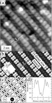 |
Figure 1: (a) Filled-state STM image acquired with a sample bias of -2.1 V measuring 11 nm X 11 nm; (b) Simulated STM image of the B2 structural model using a filled-state bias of 0.3 V below the valence band maximum; (c) B2 structural model structural model; (d) Height cross-section across a dimer trench along the [110] direction extracted from the STM image shown in (a).
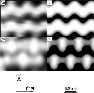 |
Figure 2: Comparison of experimental images (left column, a), c)) and theory (right column, b) d) for filled-state images of the clean Si(001) c(4x2) surface (upper row, a), b)) and after Mn deposition (lower row, c), d)). While theory and experiment are in close agreement for the same surface structure, the two structures give clearly distinct images, in both theory and experiment.
Bookmark:


|
|
||
|
|
||
| The latest news from around the world, FREE | ||
|
|
||
|
|
||
| Premium Products | ||
|
|
||
|
Only the news you want to read!
Learn More |
||
|
|
||
|
Full-service, expert consulting
Learn More |
||
|
|
||