Home > Press > University of Chicago scientists invent smallest known way to guide light: 2D optical waveguides could point way to new technology
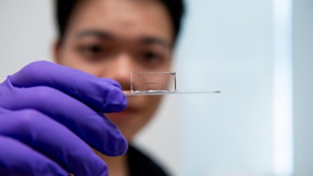 |
| Scientists at the University of Chicago found a glass crystal just a few atoms thick can trap and carry light—and could be used for applications. The material is visible as the thin line in the center of the plastic, held by study co-author Hanyu Hong. CREDIT Photo by Jean Lachat |
Abstract:
Directing light from place to the place is the backbone of our modern world. Beneath the oceans and across continents, fiber optic cables carry light that encodes everything from YouTube videos to banking transmissions—all inside strands about the size of a hair.
University of Chicago scientists invent smallest known way to guide light: 2D optical waveguides could point way to new technology
Chicago, IL | Posted on August 11th, 2023University of Chicago Prof. Jiwoong Park, however, wondered what would happen if you made even thinner and flatter strands—in effect, so thin that they’re actually 2D instead of 3D. What would happen to the light?
Through a series of innovative experiments, he and his team found that a sheet of glass crystal just a few atoms thick could trap and carry light. Not only that, but it was surprisingly efficient and could travel relatively long distances—up to a centimeter, which is very far in the world of light-based computing.
The research, published Aug. 10 in Science, demonstrates what are essentially 2D photonic circuits, and could open paths to new technology.
“We were utterly surprised by how powerful this super-thin crystal is; not only can it hold energy, but deliver it a thousand times further than anyone has seen in similar systems,” said lead study author Jiwoong Park, a professor and chair of chemistry and faculty member of the James Franck Institute and Pritzker School of Molecular Engineering. “The trapped light also behaved like it is traveling in a 2D space.”
Guiding light
The newly invented system is a way to guide light—known as a waveguide—that is essentially two-dimensional. In tests, the researchers found they could use extremely tiny prisms, lenses, and switches to guide the path of the light along a chip—all the ingredients for circuits and computations.
Photonic circuits already exist, but they are much larger and three-dimensional. Crucially, in existing waveguides, the particles of light—called photons—always travel enclosed inside the waveguide.
With this system, the scientists explained, the glass crystal is actually thinner than the photon itself—so part of the photon actually sticks out of the crystal as it travels.
It’s a bit like the difference between building a tube to send suitcases around an airport, versus setting them on top of a conveyer belt. With a conveyer belt, the suitcases are open to the air and you can easily see and adjust them en route. This approach makes it much easier to build intricate devices with the glass crystals, as the light can be easily moved with lenses or prisms.
The photons can also experience information about the conditions along the way. Think of checking the suitcases coming in from outdoors to see if it’s snowing outside. Similarly, the scientists can imagine using these waveguides to make sensors at the microscopic level.
“For example, say you had a sample of liquid, and you wanted to sense whether a particular molecule was present,” explained Park. “You could design it so that this waveguide travels through the sample, and the presence of that molecule would change how the light behaves.”
The scientists are also interested in building very thin photonic circuits which could be stacked to integrate many more tiny devices into the same chip area. The glass crystal they used in these experiments was molybdenum disulfide, but the principles should work for other materials.
Though theoretical scientists had predicted that this behavior should exist, actually realizing it in the laboratory was a years-long journey, the scientists said.
“It was a really challenging but satisfying problem, because we were walking into a completely new field. So everything we needed we had to devise ourselves—from growing the material to measuring how the light was moving,” said graduate student Hanyu Hong, the co-first author of the paper.
Myungjae Lee (formerly a postdoctoral researcher at UChicago, now faculty at Seoul National University) was the other first co-author of the paper. Postdoctoral researcher Jaehyung Yu, Fauzia Mujid (PhD’22, now at Ecolab), and graduate students Andrew Ye and Ce Liang were also authors on the paper.
The scientists used the University of Chicago Materials Research Science and Engineering Center, the fabrication facilities of the Pritzker Nanofabrication Facility, and the Cornell Center for Materials Research.
####
For more information, please click here
Contacts:
Meredith Davis
University of Chicago
Copyright © University of Chicago
If you have a comment, please Contact us.Issuers of news releases, not 7th Wave, Inc. or Nanotechnology Now, are solely responsible for the accuracy of the content.
Bookmark:


| Related Links |
| Related News Press |
News and information
![]() Quantum computer improves AI predictions April 17th, 2026
Quantum computer improves AI predictions April 17th, 2026
![]() Flexible sensor gains sensitivity under pressure April 17th, 2026
Flexible sensor gains sensitivity under pressure April 17th, 2026
![]() A reusable chip for particulate matter sensing April 17th, 2026
A reusable chip for particulate matter sensing April 17th, 2026
![]() Detecting vibrational quantum beating in the predissociation dynamics of SF6 using time-resolved photoelectron spectroscopy April 17th, 2026
Detecting vibrational quantum beating in the predissociation dynamics of SF6 using time-resolved photoelectron spectroscopy April 17th, 2026
2 Dimensional Materials
![]() Flexible sensor gains sensitivity under pressure April 17th, 2026
Flexible sensor gains sensitivity under pressure April 17th, 2026
Possible Futures
![]() A fundamentally new therapeutic approach to cystic fibrosis: Nanobody repairs cellular defect April 17th, 2026
A fundamentally new therapeutic approach to cystic fibrosis: Nanobody repairs cellular defect April 17th, 2026
![]() UC Irvine physicists discover method to reverse ‘quantum scrambling’ : The work addresses the problem of information loss in quantum computing system April 17th, 2026
UC Irvine physicists discover method to reverse ‘quantum scrambling’ : The work addresses the problem of information loss in quantum computing system April 17th, 2026
Chip Technology
![]() A reusable chip for particulate matter sensing April 17th, 2026
A reusable chip for particulate matter sensing April 17th, 2026
![]() Metasurfaces smooth light to boost magnetic sensing precision January 30th, 2026
Metasurfaces smooth light to boost magnetic sensing precision January 30th, 2026
Optical computing/Photonic computing
![]() ICFO researchers overcome long-standing bottleneck in single photon detection with twisted 2D materials August 8th, 2025
ICFO researchers overcome long-standing bottleneck in single photon detection with twisted 2D materials August 8th, 2025
![]() Programmable electron-induced color router array May 14th, 2025
Programmable electron-induced color router array May 14th, 2025
Announcements
![]() A fundamentally new therapeutic approach to cystic fibrosis: Nanobody repairs cellular defect April 17th, 2026
A fundamentally new therapeutic approach to cystic fibrosis: Nanobody repairs cellular defect April 17th, 2026
![]() UC Irvine physicists discover method to reverse ‘quantum scrambling’ : The work addresses the problem of information loss in quantum computing system April 17th, 2026
UC Irvine physicists discover method to reverse ‘quantum scrambling’ : The work addresses the problem of information loss in quantum computing system April 17th, 2026
Interviews/Book Reviews/Essays/Reports/Podcasts/Journals/White papers/Posters
![]() A fundamentally new therapeutic approach to cystic fibrosis: Nanobody repairs cellular defect April 17th, 2026
A fundamentally new therapeutic approach to cystic fibrosis: Nanobody repairs cellular defect April 17th, 2026
![]() UC Irvine physicists discover method to reverse ‘quantum scrambling’ : The work addresses the problem of information loss in quantum computing system April 17th, 2026
UC Irvine physicists discover method to reverse ‘quantum scrambling’ : The work addresses the problem of information loss in quantum computing system April 17th, 2026
Photonics/Optics/Lasers
![]() Metasurfaces smooth light to boost magnetic sensing precision January 30th, 2026
Metasurfaces smooth light to boost magnetic sensing precision January 30th, 2026
![]() From sensors to smart systems: the rise of AI-driven photonic noses January 30th, 2026
From sensors to smart systems: the rise of AI-driven photonic noses January 30th, 2026
|
|
||
|
|
||
| The latest news from around the world, FREE | ||
|
|
||
|
|
||
| Premium Products | ||
|
|
||
|
Only the news you want to read!
Learn More |
||
|
|
||
|
Full-service, expert consulting
Learn More |
||
|
|
||